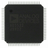
AD5522JSVDZ Analog Devices Inc, AD5522JSVDZ Datasheet - Page 53

AD5522JSVDZ
Manufacturer Part Number
AD5522JSVDZ
Description
IC, DAC, 16BIT, QFP-80
Manufacturer
Analog Devices Inc
Datasheet
1.AD5522JSVDZ.pdf
(64 pages)
Specifications of AD5522JSVDZ
Resolution (bits)
16bit
Input Channel Type
Serial
Supply Voltage Range - Digital
2.3V To 5.25V
Supply Current
36mA
Digital Ic Case Style
QFP
No. Of Pins
80
Data Interface
LVDS, Serial
Design Resources
Parametric Measurement Unit and Supporting Components for PAD Appls Using AD5522 and AD7685 (CN0104)
Lead Free Status / RoHS Status
Lead free / RoHS Compliant
Available stocks
Company
Part Number
Manufacturer
Quantity
Price
Company:
Part Number:
AD5522JSVDZ
Manufacturer:
WD
Quantity:
1 000
Company:
Part Number:
AD5522JSVDZ
Manufacturer:
Analog Devices Inc
Quantity:
10 000
Part Number:
AD5522JSVDZ
Manufacturer:
ADI/亚德诺
Quantity:
20 000
READ REGISTERS
Readback of all the registers in the device is possible via the SPI
and the LVDS interfaces. To read data from a register, it is first
necessary to write a readback command to tell the device which
register is required for readback. See Table 30 to address the
appropriate channel.
When the required channel is addressed, the device loads
the 24-bit readback data into the MSB positions of the 29-bit
serial shift register (the five LSBs are filled with 0s). SCLK rising
edges clock this readback data out on SDO (framed by the
SYNC signal).
Table 30. Read Functions of the AD5522
B28
RD/WR
Read Functions
1
1
1
1
Read Addressed PMU Register (Only One PMU Register Can Be Read at One Time)
1
1
1
1
Read Addressed DAC M Register (Only One DAC Register Can Be Read at One Time)
1
1
1
1
Read Addressed DAC C Register (Only One DAC Register Can Be Read at One Time)
1
1
1
1
Read Addressed DAC X1 Register (Only One DAC Register Can Be Read at One Time)
1
1
1
1
B27
PMU3
0
0
0
0
0
0
0
1
0
0
0
1
0
0
0
1
0
0
0
1
B26
PMU2
0
0
0
0
0
0
1
0
0
0
1
0
0
0
1
0
0
0
1
0
B25
PMU1
0
0
0
0
0
1
0
0
0
1
0
0
0
1
0
0
0
1
0
0
B24
PMU0
0
0
0
0
1
0
0
0
1
0
0
0
1
0
0
0
1
0
0
0
B23
MODE1
0
0
1
1
0
0
0
0
0
0
0
0
1
1
1
1
1
1
1
1
Rev. D | Page 53 of 64
B22
MODE0
0
1
0
1
0
0
0
0
1
1
1
1
0
0
0
0
1
1
1
1
A minimum of 24 clock rising edges is required to shift the
readback data out of the shift register. If writing a 24-bit word to
shift data out of the device, the user must ensure that the 24-bit
write is effectively an NOP (no operation) command. The last
five bits in the shift register are always 00000: these five bits
become the MSBs of the shift register when the 24-bit write is
loaded. To ensure that the device receives an NOP command as
described in Table 20, the recommended flush command is
0xFFFFFF; thus, no change is made to any register in the device.
Readback data can also be shifted out by writing another 29-bit
write or read command. If writing a 29-bit command, the read-
back data is MSB data available on SDO, followed by 00000.
B21 to B0
Data bits
All 0s
All 0s
X (don’t care)
All 0s
All 0s
DAC address
(see Table 29)
DAC address
(see Table 29)
DAC address
(see Table 29)
CH3
Read from system control register
Read from comparator status register
Reserved
Read from alarm status register
CH3
CH3
CH3
CH3
CH2
CH2
CH2
CH2
CH2
Selected Channel
CH1
CH1
CH1
CH1
CH1
AD5522
CH0
CH0
CH0
CH0
CH0


