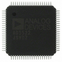
AD5522JSVDZ Analog Devices Inc, AD5522JSVDZ Datasheet - Page 38

AD5522JSVDZ
Manufacturer Part Number
AD5522JSVDZ
Description
IC, DAC, 16BIT, QFP-80
Manufacturer
Analog Devices Inc
Datasheet
1.AD5522JSVDZ.pdf
(64 pages)
Specifications of AD5522JSVDZ
Resolution (bits)
16bit
Input Channel Type
Serial
Supply Voltage Range - Digital
2.3V To 5.25V
Supply Current
36mA
Digital Ic Case Style
QFP
No. Of Pins
80
Data Interface
LVDS, Serial
Design Resources
Parametric Measurement Unit and Supporting Components for PAD Appls Using AD5522 and AD7685 (CN0104)
Lead Free Status / RoHS Status
Lead free / RoHS Compliant
Available stocks
Company
Part Number
Manufacturer
Quantity
Price
Company:
Part Number:
AD5522JSVDZ
Manufacturer:
WD
Quantity:
1 000
Company:
Part Number:
AD5522JSVDZ
Manufacturer:
Analog Devices Inc
Quantity:
10 000
Part Number:
AD5522JSVDZ
Manufacturer:
ADI/亚德诺
Quantity:
20 000
AD5522
Table 14. References Suggested For Use with AD5522
Part No.
ADR435
ADR445
ADR431
ADR441
1
For other voltage and current ranges, the required reference
level can be calculated as follows:
1.
2.
3.
4.
5.
Reference Selection Example
If, given the following conditions:
Nominal output range = 10 V (−2 V to +8 V)
Offset error = ±100 mV
Gain error = ±0.5%
REFGND = AGND = 0 V
Then, with gain error = ±0.5%, the maximum positive gain
error = +0.5%, and the output range including gain error =
10 V + 0.005(10 V) = 10.05 V.
With offset error = ±100 mV, the maximum offset error span =
2(100 mV) = 0.2 V, and the output range including gain error
and offset error = 10.05 V + 0.2 V = 10.25 V.
To calculate VREF with actual output range = 10.25 V, that is,
−2.125 V to +8.125 V (centered),
If the solution yields an inconvenient reference level, the user
can adopt one of the following approaches:
•
•
•
Subset of the possible references suitable for use with the AD5522. Visit www.analog.com for more options.
Identify the nominal range required.
Identify the maximum offset span and the maximum gain
required on the full output signal range.
Calculate the new maximum output range, including the
expected maximum gain and offset errors.
Choose the new required VOUT
the VOUT limits centered on the nominal values. Note that
AVDD and AVSS must provide sufficient headroom.
Calculate the value of VREF as follows:
VREF = (VOUT
VREF = (8.125 V + 2.125 V)/4.5 = 2.28 V
Use a resistor divider to divide down a convenient, higher
reference level to the required level.
Select a convenient reference level above VREF and modify
the gain and offset registers to digitally downsize the reference.
In this way, the user can use almost any convenient refer-
ence level.
Use a combination of these two approaches.
Voltage (V)
5
5
2.5
2.5
MAX
− VOUT
MIN
±0.04
±0.04
±0.04
±0.04
Initial
Accuracy %
)/4.5
MAX
and VOUT
MIN
Ref Out
TC (ppm/°C)
1
1
1
1
, keeping
1
Rev. D | Page 38 of 64
In this case, the optimum reference is a 2.5 V reference; the user
can use the M and C registers and the offset DAC to achieve the
required −2 V to +8 V range. Change the I
5 to ensure a full-scale current range of the specified values (see
the Current Range Selection section). This gain also allows opti-
mization of power supplies and minimizes power consumption
within the device.
It is important to bear in mind when choosing a reference value
that values other than 5 V (MI gain = 10) and 2.5 V (MI gain = 5)
result in current ranges other than those specified. See the
Measure Current Gains section for more details.
CALIBRATION
Calibration involves determining the gain and offset of each
channel in each mode and overwriting the default values in the
M and C registers of the individual DACs. In some cases (for
example, FI mode), the calibration constants, particularly those
for gains, may be range dependent.
Reducing Zero-Scale Error
Zero-scale error can be reduced as follows:
1.
2.
3.
Reducing Gain Error
Gain error can be reduced as follows:
1.
2.
3.
4.
Ref Output
Current (mA)
30
10
30
10
Set the output to the lowest possible value.
Measure the actual output voltage and compare it to the
required value. This gives the zero-scale error.
Calculate the number of LSBs equivalent to the zero-scale
error and add/subtract this number to the default value of
the C register.
Measure the zero-scale error.
Set the output to the highest possible value.
Measure the actual output voltage and compare it to the
required value. This is the gain error.
Calculate the number of LSBs equivalent to the gain error
and subtract this number from the default value of the M
register. Note that only positive gain error can be reduced.
Supply Voltage
Range (V)
+7 to +18
+5.5 to +18
+4.5 to +18
+3 to +18
SENSE
amplifier gain to
Package
MSOP, SOIC
MSOP, SOIC
MSOP, SOIC
MSOP, SOIC


