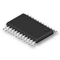
PCA9555PW NXP Semiconductors, PCA9555PW Datasheet - Page 14

PCA9555PW
Manufacturer Part Number
PCA9555PW
Description
IC, I2C-BUS AND SMBUS I/O PORT, TSSOP24
Manufacturer
NXP Semiconductors
Datasheet
1.PCA9555BS118.pdf
(34 pages)
Specifications of PCA9555PW
Chip Configuration
16 Bit
Bus Frequency
400kHz
Ic Interface Type
I2C
No. Of I/o's
16
Supply Voltage Range
2.3V To 5.5V
Digital Ic Case Style
TSSOP
No. Of Pins
24
Termination Type
SMD
Filter Terminals
SMD
Rohs Compliant
Yes
Lead Free Status / RoHS Status
Lead free / RoHS Compliant
Available stocks
Company
Part Number
Manufacturer
Quantity
Price
Company:
Part Number:
PCA9555PW
Manufacturer:
NXP
Quantity:
3 125
Company:
Part Number:
PCA9555PW
Manufacturer:
NXP Semiconductors
Quantity:
36 610
Part Number:
PCA9555PW
Manufacturer:
PHILIPS
Quantity:
20 000
Company:
Part Number:
PCA9555PW/G
Manufacturer:
MPS
Quantity:
23 062
Part Number:
PCA9555PW/G118
Manufacturer:
PHILIPS/飞利浦
Quantity:
20 000
Part Number:
PCA9555PWR
Manufacturer:
TI/德州仪器
Quantity:
20 000
Part Number:
PCA9555PWRG4
Manufacturer:
TI/德州仪器
Quantity:
20 000
NXP Semiconductors
7. Characteristics of the I
PCA9555_8
Product data sheet
6.5.3 Interrupt output
7.1.1 START and STOP conditions
7.1 Bit transfer
The open-drain interrupt output is activated when one of the port pins changes state and
the pin is configured as an input. The interrupt is deactivated when the input returns to its
previous state or the Input Port register is read (see
output cannot cause an interrupt. Since each 8-bit port is read independently, the interrupt
caused by Port 0 will not be cleared by a read of Port 1 or the other way around.
Remark: Changing an I/O from an output to an input may cause a false interrupt to occur
if the state of the pin does not match the contents of the Input Port register.
The I
lines are a serial data line (SDA) and a serial clock line (SCL). Both lines must be
connected to a positive supply via a pull-up resistor when connected to the output stages
of a device. Data transfer may be initiated only when the bus is not busy.
One data bit is transferred during each clock pulse. The data on the SDA line must remain
stable during the HIGH period of the clock pulse as changes in the data line at this time
will be interpreted as control signals (see
Both data and clock lines remain HIGH when the bus is not busy. A HIGH-to-LOW
transition of the data line while the clock is HIGH is defined as the START condition (S). A
LOW-to-HIGH transition of the data line while the clock is HIGH is defined as the STOP
condition (P) (see
Fig 15. Bit transfer
Fig 16. Definition of START and STOP conditions
2
C-bus is for 2-way, 2-line communication between different ICs or modules. The two
SDA
SCL
START condition
2
SDA
SCL
Figure
C-bus
S
Rev. 08 — 22 October 2009
16).
data valid
data line
stable;
16-bit I
Figure
2
allowed
change
of data
C-bus and SMBus I/O port with interrupt
15).
Figure
13). A pin configured as an
STOP condition
mba607
P
PCA9555
© NXP B.V. 2009. All rights reserved.
mba608
14 of 34


