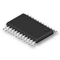
PCA9555PW NXP Semiconductors, PCA9555PW Datasheet - Page 9

PCA9555PW
Manufacturer Part Number
PCA9555PW
Description
IC, I2C-BUS AND SMBUS I/O PORT, TSSOP24
Manufacturer
NXP Semiconductors
Datasheet
1.PCA9555BS118.pdf
(34 pages)
Specifications of PCA9555PW
Chip Configuration
16 Bit
Bus Frequency
400kHz
Ic Interface Type
I2C
No. Of I/o's
16
Supply Voltage Range
2.3V To 5.5V
Digital Ic Case Style
TSSOP
No. Of Pins
24
Termination Type
SMD
Filter Terminals
SMD
Rohs Compliant
Yes
Lead Free Status / RoHS Status
Lead free / RoHS Compliant
Available stocks
Company
Part Number
Manufacturer
Quantity
Price
Company:
Part Number:
PCA9555PW
Manufacturer:
NXP
Quantity:
3 125
Company:
Part Number:
PCA9555PW
Manufacturer:
NXP Semiconductors
Quantity:
36 610
Part Number:
PCA9555PW
Manufacturer:
PHILIPS
Quantity:
20 000
Company:
Part Number:
PCA9555PW/G
Manufacturer:
MPS
Quantity:
23 062
Part Number:
PCA9555PW/G118
Manufacturer:
PHILIPS/飞利浦
Quantity:
20 000
Part Number:
PCA9555PWR
Manufacturer:
TI/德州仪器
Quantity:
20 000
Part Number:
PCA9555PWRG4
Manufacturer:
TI/德州仪器
Quantity:
20 000
NXP Semiconductors
PCA9555_8
Product data sheet
6.5.1 Writing to the port registers
6.5 Bus transactions
Data is transmitted to the PCA9555 by sending the device address and setting the least
significant bit to a logic 0 (see
sent after the address and determines which register will receive the data following the
command byte.
The eight registers within the PCA9555 are configured to operate as four register pairs.
The four pairs are Input Ports, Output Ports, Polarity Inversion Ports, and Configuration
Ports. After sending data to one register, the next data byte will be sent to the other
register in the pair (see
Output Port 1 (register 3), then the next byte will be stored in Output Port 0 (register 2).
There is no limitation on the number of data bytes sent in one write transmission. In this
way, each 8-bit register may be updated independently of the other registers.
Fig 9.
configuration
write polarity
shift register
shift register
shift register
write pulse
read pulse
data from
data from
data from
pulse
pulse
write
At power-on reset, all registers return to default values.
Simplified schematic of I/Os
configuration
register
D
CK
FF
Q
Q
Rev. 08 — 22 October 2009
Figure 10
Figure 8 “PCA9555 device
output port
register
D
CK
FF
and
Q
16-bit I
Figure
input port
register
polarity inversion
register
D
CK
D
CK
2
11). For example, if the first byte is sent to
C-bus and SMBus I/O port with interrupt
FF
FF
Q
Q
address”). The command byte is
Q1
Q2
100 k
PCA9555
© NXP B.V. 2009. All rights reserved.
output port
register data
V
I/O pin
V
input port
register data
to INT
polarity
inversion
register data
DD
SS
002aac703
9 of 34


