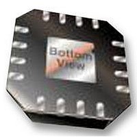
ADN2531ACPZ-R2 Analog Devices Inc, ADN2531ACPZ-R2 Datasheet - Page 11

ADN2531ACPZ-R2
Manufacturer Part Number
ADN2531ACPZ-R2
Description
IC, LASER DIODE DRIVER, 11.3GBPS LFCSP16
Manufacturer
Analog Devices Inc
Datasheet
1.ADN2531ACPZ-R7.pdf
(20 pages)
Specifications of ADN2531ACPZ-R2
Laser Driver Type
Laser Diode
Supply Current
36mA
Bias Current
100mA
Modulation Current
70mA
Data Rate
11.3Gbps
Supply Voltage Range
3V To 3.6V
Driver Case Style
LFCSP
No. Of Pins
16
Lead Free Status / RoHS Status
Lead free / RoHS Compliant
THEORY OF OPERATION
As shown in Figure 1, the ADN2531 consists of an input stage and
two voltage-controlled current sources for bias and modulation.
The bias current is available at the IBIAS pin. It is controlled by the
voltage at the BSET pin and can be monitored at the IBMON pin.
The differential modulation current is available at the IMODP
and IMODN pins. It is controlled by the voltage at the MSET pin.
The output stage implements the active back-termination
circuitry for proper transmission line matching and power
consumption reduction. The ADN2531 can drive a load with
differential resistance ranging from 5 Ω to 140 Ω. The excellent
back-termination in the ADN2531 absorbs signal reflections
from the TOSA end of the output transmission lines, enabling
excellent optical eye quality to be achieved even when the
TOSA end of the output transmission lines is significantly
misterminated.
INPUT STAGE
The input stage of the ADN2531 converts the data signal applied
to the DATAP and DATAN pins to a level that ensures proper
operation of the high speed switch. The equivalent circuit of the
input stage is shown in Figure 23.
The DATAP and DATAN pins are terminated internally with a
100 Ω differential termination resistor. This minimizes signal
reflections at the input that could otherwise lead to degradation
in the output eye diagram. It is not recommended to drive the
ADN2531 with single-ended data signal sources.
The ADN2531 input stage must be ac-coupled to the signal source
to eliminate the need for matching between the common-mode
voltages of the data signal source and the input stage of the driver
(see Figure 24). The ac coupling capacitors should have an
impedance less than 50 Ω over the required frequency range.
Generally, this is achieved using 10 nF to 100 nF capacitors, for
more than 1 Gbps operation.
DATAN
DATAP
Figure 23. Equivalent Circuit of the Input Stage
V
CC
50Ω
50Ω
V
CC
Rev. 0 | Page 11 of 20
BIAS CURRENT
The bias current is generated internally using a voltage-to-current
converter consisting of an internal operational amplifier and a
transistor, as shown in Figure 25.
The BSET to I
at 100 mA/V by the internal resistors, and the bias current is
monitored at the IBMON pin using a current mirror with a gain
equal to 1/100. By connecting a 750 Ω resistor between IBMON
and GND, the bias current can be monitored as a voltage across
the resistor. A low temperature coefficient precision resistor must
be used for the IBMON resistor (R
of R
contributes to the overall error budget for the I
If the IBMON voltage is being connected to an ADC for analog-
to-digital conversion, R
minimize errors due to voltage drops on the ground plane. See the
Design Example section for example calculations of the accuracy of
the I
Figure 24. AC Coupling the Data Source to the ADN2531 Data Inputs
IBMON
BIAS
Figure 25. Voltage-to-Current Converter Used to Generate I
monitor as a percentage of the nominal I
DATA SIGNAL SOURCE
BSET
due to tolerances or drift in its value over temperature
50Ω
BIAS
ADN2531
voltage-to-current conversion factor is set
800Ω
200Ω
50Ω
IBMON
GND
should be placed close to the ADC to
200Ω
C
C
V
CC
IBMON
2Ω
). Any error in the value
DATAP
DATAN
I
I
BMON
BIAS
ADN2531
BIAS
monitor voltage.
IBMON
IBIAS
BIAS
ADN2531
value.
BIAS


