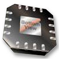
ADN2531ACPZ-R2 Analog Devices Inc, ADN2531ACPZ-R2 Datasheet - Page 3

ADN2531ACPZ-R2
Manufacturer Part Number
ADN2531ACPZ-R2
Description
IC, LASER DIODE DRIVER, 11.3GBPS LFCSP16
Manufacturer
Analog Devices Inc
Datasheet
1.ADN2531ACPZ-R7.pdf
(20 pages)
Specifications of ADN2531ACPZ-R2
Laser Driver Type
Laser Diode
Supply Current
36mA
Bias Current
100mA
Modulation Current
70mA
Data Rate
11.3Gbps
Supply Voltage Range
3V To 3.6V
Driver Case Style
LFCSP
No. Of Pins
16
Lead Free Status / RoHS Status
Lead free / RoHS Compliant
SPECIFICATIONS
V
Typical values are specified at 25°C and I
Table 1.
Parameter
BIAS CURRENT (I
MODULATION CURRENT (IMODP, IMODN)
DATA INPUTS (DATAP, DATAN)
BIAS CONTROL INPUT (BSET)
MODULATION CONTROL INPUT (MSET)
BIAS MONITOR (IBMON)
AUTOMATIC LASER SHUTDOWN (ALS)
CC
Accuracy of I
Bias Current Range
Bias Current While ALS Asserted
Compliance Voltage
Modulation Current I
I
Crosspoint Adjust (CPA) Range
Rise Time (20% to 80%)
Fall Time (20% to 80%)
Random Jitter
Deterministic Jitter
Deterministic Jitter
Differential |S22|
Compliance Voltage
Input Data Rate
Differential Input Swing
Differential |S11|
Input Termination Resistance
BSET Voltage to I
BSET Input Resistance
MSET Voltage to I
MSET Input Resistance
I
V
V
I
I
ALS Assert Time
ALS Negate Time
MOD
BMON
IL
IH
IH
IL
= VCC
While ALS Asserted
to I
BIAS
MIN
Ratio
to VCC
BIAS
BIAS
2, 3, 4
to I
)
BIAS
MOD
2, 4, 5
BMON
2, 4, 6
1
Gain
MAX
1
MOD
Gain
2, 3, 4
2, 3, 4
, T
Ratio
Range
A
= −40°C to +100°C, 12 Ω differential load impedance, crosspoint adjust disabled, unless otherwise noted.
2
BIAS
= I
0.6
0.55
35
V
0.15
−5.0
−4.0
−2.5
−2
2.0
−20
0
Min
10
10
85
800
MOD
CC
− 1.1
= 40 mA with crosspoint adjust disabled, unless otherwise noted.
Typ
70
26
26
<0.5
5.4
5.8
5.4
5.8
−5
−10.5
−15
100
100
1000
120
600
10
Rev. 0 | Page 3 of 20
Max
100
300
V
V
80
500
65
32.5
32.5
8.2
8.2
8.2
8.2
V
11.3
1.6
115
1200
+5.0
+4.0
+2.5
+2
0.8
+20
200
2
10
CC
CC
CC
+ 1.1
dB
Unit
mA
μA
V
V
mA diff
mA diff
μA diff
%
ps
ps
ps rms
ps p-p
ps p-p
ps p-p
ps p-p
dB
V
Gbps
V p-p diff
dB
Ω
mA/V
Ω
mA/V
Ω
μA/mA
%
%
%
%
V
V
μA
μA
μs
μs
Test Conditions/Comments
ALS = high
I
I
R
R
ALS = high
10.7 Gbps, CPA disabled
10.7 Gbps, CPA 35% to 65%
11.3 Gbps, CPA disabled
11.3 Gbps, CPA 35% to 65%
5 GHz < f < 10 GHz, Z
f < 5 GHz, Z
NRZ
Differential ac-coupled
f < 10 GHz, Z
Differential
10 mA ≤ I
20 mA ≤ I
40 mA ≤ I
70 mA ≤ I
Rising edge of ALS to falling edge of I
I
Falling edge of ALS to rising edge of I
I
BIAS
BIAS
MOD
MOD
LOAD
LOAD
= 80 mA
= 10 mA
below 10% of nominal; see Figure 2
above 90% of nominal; see Figure 2
= 5 Ω to 50 Ω differential
= 100 Ω differential
BIAS
BIAS
BIAS
BIAS
0
= 100 Ω differential
0
< 20 mA, R
< 40 mA, R
< 70 mA, R
< 80 mA, R
= 100 Ω differential
0
= 100 Ω differential
IBMON
IBMON
IBMON
IBMON
= 750 Ω
= 750 Ω
= 750 Ω
= 750 Ω
ADN2531
7
BIAS
BIAS
and
and
7


