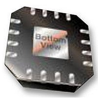
ADN2531ACPZ-R2 Analog Devices Inc, ADN2531ACPZ-R2 Datasheet - Page 13

ADN2531ACPZ-R2
Manufacturer Part Number
ADN2531ACPZ-R2
Description
IC, LASER DIODE DRIVER, 11.3GBPS LFCSP16
Manufacturer
Analog Devices Inc
Datasheet
1.ADN2531ACPZ-R7.pdf
(20 pages)
Specifications of ADN2531ACPZ-R2
Laser Driver Type
Laser Diode
Supply Current
36mA
Bias Current
100mA
Modulation Current
70mA
Data Rate
11.3Gbps
Supply Voltage Range
3V To 3.6V
Driver Case Style
LFCSP
No. Of Pins
16
Lead Free Status / RoHS Status
Lead free / RoHS Compliant
The equivalent circuits for the MSET, IMODP, and IMODN pins
are shown in Figure 32 and Figure 33. The two 50 Ω resistors in
Figure 33 represent the active back-termination resistance.
The recommended configuration of the MSET, IMODP, and
IMODN pins is shown in Figure 34. See Table 6 for recom-
mended components. When the voltage on DATAP is greater
than the voltage on DATAN, the modulation current flows into
the IMODP pin and out of the IMODN pin, generating an
optical Logic 1 level at the TOSA output when the TOSA is
connected as shown in Figure 34.
The ratio between the voltage applied to the MSET pin and the
differential modulation current available at the IMODP and
IMODN pins is a function of the load resistance value, as shown
in Figure 35.
V
MSET
Figure 33. Equivalent Circuit of the IMODP and IMODN Pins
Figure 34. Recommended Configuration for the
MSET
Figure 32. Equivalent Circuit of the MSET Pin
MSET
ADN2531
V
CC
GND
50Ω
MSET, IMODP, and IMODN Pins
IMODN
IMODP
IBIAS
IMODN
V
CC
7.7Ω
400Ω
200Ω
Z
Z
Z
L
0
0
7.7Ω
= 100Ω
= 25Ω
= 25Ω
IMODP
V
V
V
L
L
CC
CC
CC
50Ω
C
C
V
CC
Z
Z
0
0
= 25Ω
= 25Ω
L
L
V
CC
FP/DFB
TOSA
Rev. 0 | Page 13 of 20
Using the resistance of the TOSA, the user can calculate the
voltage range that should be applied to the MSET pin to
generate the required modulation current range (see the
example in the Applications Information section).
The circuit used to drive the MSET voltage must be able to
drive the 600 Ω resistance of the MSET pin. To be able to drive
80 mA modulation currents through the differential load, the
output stage of the ADN2531 (IMODP and IMODN pins) must
be ac-coupled to the load. The voltages at these pins have a dc
component equal to V
peak-to-peak amplitude of I
load impedance (R
the transmission line characteristic impedance sets the peak-to-
peak amplitude. For the case where R
the single-ended, peak-to-peak amplitude is I
For proper operation of the output stage, the voltages at the
IMODP and IMODN pins must be between the compliance
voltage specifications for this pin over supply, temperature, and
modulation current range, as shown in Figure 36. See the
Headroom Calculations section for examples of headroom
calculations.
Figure 36. Allowable Range for the Voltage at IMODP and IMODN
200
190
180
170
160
150
140
130
120
110
100
90
80
70
60
50
Figure 35. MSET Voltage to Modulation Current Ratio vs.
0
V
V
CC
CC
+ 1.1V
– 1.1V
V
CC
10
TOSA
V
Differential Load Resistance
IMODP,
CC
) is less than 100 Ω differential because
and an ac component with single-ended
DIFFERENTIAL R
20
V
MOD
IMODN
MAXIMUM
TYPICAL
MINIMUM
NORMAL OPERATION REGION
× 50 Ω. This is the case when the
30
LOAD
TOSA
40
(Ω)
is greater than 100 Ω,
MOD
× R
50
ADN2531
TOSA
÷ 2.
60


