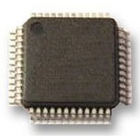
PCA9626B NXP Semiconductors, PCA9626B Datasheet - Page 23

PCA9626B
Manufacturer Part Number
PCA9626B
Description
IC, LED DRIVER, RGBA, 48-LQFP
Manufacturer
NXP Semiconductors
Datasheet
1.PCA9626B118.pdf
(47 pages)
Specifications of PCA9626B
No. Of Outputs
24
Output Current
100mA
Output Voltage
40V
Input Voltage
2.3V To 5.5V
Dimming Control Type
PWM
Driver Case Style
LQFP
Switching Frequency
1MHz
Base Number
9626
Operating
RoHS Compliant
Led Driver Application
RGB Or RGBA LED Drivers, LED Status Information, Displays, Backlights
Rohs Compliant
Yes
Lead Free Status / Rohs Status
Details
Available stocks
Company
Part Number
Manufacturer
Quantity
Price
Part Number:
PCA9626B
Manufacturer:
NXP/恩智浦
Quantity:
20 000
Company:
Part Number:
PCA9626B,118
Manufacturer:
NXP Semiconductors
Quantity:
10 000
Part Number:
PCA9626B,118
Manufacturer:
NXP/恩智浦
Quantity:
20 000
Company:
Part Number:
PCA9626B/S911
Manufacturer:
FREESCALE
Quantity:
430
Part Number:
PCA9626BS
Manufacturer:
NXP/恩智浦
Quantity:
20 000
Company:
Part Number:
PCA9626BЈ¬118
Manufacturer:
PH3
Quantity:
90
NXP Semiconductors
PCA9626_2
Product data sheet
7.3.8 SUBADR1 to SUBADR3, I
7.3.9 ALLCALLADR, LED All Call I
Table 13.
Legend: * default value.
Subaddresses are programmable through the I
E4h, E8h, and the device(s) will not acknowledge these addresses right after power-up
(the corresponding SUBx bit in MODE1 register is equal to 0).
Once subaddresses have been programmed to their right values, SUBx bits need to be
set to logic 1 in order to have the device acknowledging these addresses (MODE1
register).
Only the 7 MSBs representing the I
register is a read-only bit (0).
When SUBx is set to logic 1, the corresponding I
either an I
Table 14.
Legend: * default value.
The LED All Call I
at the same time (ALLCALL bit in register MODE1 must be equal to logic 1 (power-up
default state)). This address is programmable through the I
either an I
as a Sub Call.
Only the 7 MSBs representing the All Call I
ALLCALLADR register is a read-only bit (0).
If ALLCALL bit = 0, the device does not acknowledge the address programmed in register
ALLCALLADR.
Address
23h
24h
25h
Address
26h
2
2
Register
SUBADR1
SUBADR2
SUBADR3
Register
ALLCALLADR
SUBADR1 to SUBADR3 - I
bit description
ALLCALLADR - LED All Call I
description
C-bus read or write sequence.
C-bus read or write sequence. The register address can also be programmed
2
C-bus address allows all the PCA9626s on the bus to be programmed
Rev. 02 — 31 August 2009
Bit
7:1
0
7:1
0
7:1
0
Bit
7:1
0
2
C-bus subaddress 1 to 3
Symbol
A1[7:1]
A1[0]
A2[7:1]
A2[0]
A3[7:1]
A3[0]
Symbol
AC[7:1]
AC[0]
2
C-bus address
2
2
C-bus subaddress are valid. The LSB in SUBADRx
C-bus subaddress registers 0 to 3 (address 23h to 25h)
2
C-bus address register (address 26h) bit
Access Value
R/W
R only
R/W
R only
R/W
R only
2
24-bit Fm+ I
Access Value
R/W
R only
C-bus address are valid. The LSB in
2
C-bus. Default power-up values are E2h,
2
C-bus subaddress can be used during
1110 001*
0*
1110 010*
0*
1110 100*
0*
1110 000*
0*
2
C-bus 100 mA 40 V LED driver
2
C-bus and can be used during
Description
I
reserved
I
reserved
I
reserved
2
2
2
Description
ALLCALL I
address register
reserved
C-bus subaddress 1
C-bus subaddress 2
C-bus subaddress 3
PCA9626
© NXP B.V. 2009. All rights reserved.
2
C-bus
23 of 47


