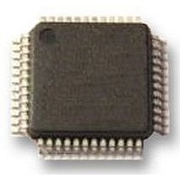
PCA9626B NXP Semiconductors, PCA9626B Datasheet - Page 25

PCA9626B
Manufacturer Part Number
PCA9626B
Description
IC, LED DRIVER, RGBA, 48-LQFP
Manufacturer
NXP Semiconductors
Datasheet
1.PCA9626B118.pdf
(47 pages)
Specifications of PCA9626B
No. Of Outputs
24
Output Current
100mA
Output Voltage
40V
Input Voltage
2.3V To 5.5V
Dimming Control Type
PWM
Driver Case Style
LQFP
Switching Frequency
1MHz
Base Number
9626
Operating
RoHS Compliant
Led Driver Application
RGB Or RGBA LED Drivers, LED Status Information, Displays, Backlights
Rohs Compliant
Yes
Lead Free Status / Rohs Status
Details
Available stocks
Company
Part Number
Manufacturer
Quantity
Price
Part Number:
PCA9626B
Manufacturer:
NXP/恩智浦
Quantity:
20 000
Company:
Part Number:
PCA9626B,118
Manufacturer:
NXP Semiconductors
Quantity:
10 000
Part Number:
PCA9626B,118
Manufacturer:
NXP/恩智浦
Quantity:
20 000
Company:
Part Number:
PCA9626B/S911
Manufacturer:
FREESCALE
Quantity:
430
Part Number:
PCA9626BS
Manufacturer:
NXP/恩智浦
Quantity:
20 000
Company:
Part Number:
PCA9626BЈ¬118
Manufacturer:
PH3
Quantity:
90
NXP Semiconductors
PCA9626_2
Product data sheet
Fig 7.
1
1
Brightness Control signal (LEDn)
Group Dimming signal
resulting Brightness + Group Dimming signal
2
2
(GRPPWM Register)
M
Minimum pulse width for LEDn Brightness Control is 40 ns.
Minimum pulse width for Group Dimming is 20.48 s.
When M = 1 (GRPPWM register value), the resulting LEDn Brightness Control + Group Dimming signal will have 2 pulses of
the LED Brightness Control signal (pulse width = N
This resulting Brightness + Group Dimming signal above shows a resulting Control signal with M = 4 (8 pulses).
Brightness + Group Dimming signals
with M = (0 to 255)
3
3
256
4
4
7.7 Individual brightness control with group dimming/blinking
2
5
5
40 ns
6
6
The I
a ‘SWRST Call Abort’. The PCA9626 does not initiate a reset of its registers. This
happens only when the format of the SWRST Call sequence is not correct.
A 97 kHz fixed frequency signal with programmable duty cycle (8 bits, 256 steps) is used
to control individually the brightness for each LED.
On top of this signal, one of the following signals can be superimposed (this signal can be
applied to the 4 LED outputs):
7
7
5. Once the right 2 bytes (SWRST data byte 1 and byte 2 only) have been sent and
•
•
256
8
8
b. Byte 2 = 5Ah: the PCA9626 acknowledges this value only. If byte 2 is not equal to
If more than 2 bytes of data are sent, the PCA9626 does not acknowledge any more.
correctly acknowledged, the master sends a STOP command to end the SWRST Call:
the PCA9626 then resets to the default value (power-up value) and is ready to be
addressed again within the specified bus free time (t
A lower 190 Hz fixed frequency signal with programmable duty cycle (8 bits,
256 steps) is used to provide a global brightness control.
A programmable frequency signal from 24 Hz to
programmable duty cycle (8 bits, 256 steps) is used to provide a global blinking
control.
2
9 10 11 12
C-bus master must interpret a non-acknowledge from the PCA9626 (at any time) as
2
5Ah, then the PCA9626 does not acknowledge it.
256
40 ns = 5.24 ms (190.7 Hz)
Rev. 02 — 31 August 2009
256
(97.6 kHz)
40 ns = 10.24 s
40 ns, with ‘N’ defined in PWMx register).
N
with N = (0 to 255)
(PWMx Register)
40 ns
507
508
509
24-bit Fm+ I
510
511
512
1
10.73
1
1
2
BUF
C-bus 100 mA 40 V LED driver
2
2
Hz (8 bits, 256 steps) with
).
3
3
4
4
5
5
6
6
PCA9626
© NXP B.V. 2009. All rights reserved.
7
7
8
8
9 10 11
002aab417
25 of 47


