OX16C950-TQBG OXFORD SEMICONDUCTOR, OX16C950-TQBG Datasheet
OX16C950-TQBG
Specifications of OX16C950-TQBG
Available stocks


Related parts for OX16C950-TQBG

OX16C950-TQBG Summary of contents
Page 1
... Sleep mode (low operating current) • System clock MHz (at 5V), 50 MHz at 3.3V • 44 PLCC and 48 TQFP packages • 5 volts operation (PLCC), 3.3/ 5V operation TQFP © Oxford Semiconductor 2005 External–Free Release OX16C950 rev B DS-0031 Sep 05 Part Nos. OX16C950-PCC60-B OX16C950-TQC60-B OX16C950-PLBG OX16C950-TQBG ...
Page 2
... RS232/RS422/RS485 interfaces. Fabricated in 0.6μm process, OX16C950 also has a low operating current and sleep mode for battery powered applications. © Oxford Semiconductor 2005 External–Free Release OX16C950 rev B DS-0031 Sep 05 Part Nos. OX16C950-PCC60-B OX16C950-TQC60-B OX16C950-PLBG OX16C950-TQBG ...
Page 3
... F C UTOMATIC UT OF BAND LOW 14 BAUD RATE GENERATION.................................................................................................................................................... 31 14 .......................................................................................................................................................... 31 ENERAL PERATION 14 ‘CPR’.................................................................................................................................... 32 LOCK RESCALER EGISTER 14 ‘TCR’............................................................................................................................................. 32 IMES LOCK EGISTER 14 ........................................................................................................................................................ 34 NPUT LOCK PTIONS 14.5 TTL C M ........................................................................................................................................................... 34 LOCK ODULE DS-0031 Sep 05 ................................................................................................................................... 30 ........................................................................................................................... 30 ONTROL External—Free Release OX16C950 rev B Page 3 ...
Page 4
... PACKAGE INFORMATION...................................................................................................................................................... 47 21 ORDERING INFORMATION .................................................................................................................................................... 48 NOTES............................................................................................................................................................................................ 49 CONTACT DETAILS...................................................................................................................................................................... EVISION ISTORY REV DATE REASON FOR CHANGE / SUMMARY OF CHANGE Sep 2005 30/8/2005 Revision for additional green order code for both TQFP & PLCC packages DS-0031 Sep 05 ‘RTL’ ....................................................................................................................... 37 ...................................................................................................................................... 37 External—Free Release OX16C950 rev B Page 4 ...
Page 5
... OXFORD SEMICONDUCTOR LTD. DS-0031 Sep 05 External—Free Release OX16C950 rev B Page 5 ...
Page 6
... Software reset Device ID 9-bit data frames RS485 buffer enable Infra-red (IrDA) Table 1 OX16C950 performance compared with 16C450, 16C550, 16C650 and 16C750 devices Improvements of the OX16C950 over previous generations of PC UART: Deeper FIFOs: OX16C950 offers 128-byte deep FIFOs for the transmitter and receiver. ...
Page 7
... OX16C950 device to software drivers. Infra-red ‘IrDA’ interface: The UART contains an IrDA compliant modulator and demodulator. 9-bit data framing: The OX16C950 may be configured to use in 9-bit character framing for multi-drop protocols where a tag ID (9 differentiates address and data characters. Control and Status ...
Page 8
... CS1 10 CS2# 11 BDOUT# 12 DS-0031 Sep 05 44 Pin Plastic Leaded Chip Carrier OX16C950-PCC60 Pin Thin Quad Flat Pack OX16C950-TQC60-B OX16C950-TQC60 External—Free Release OX16C950 rev RESET 38 OUT1# 37 DTR# 36 RTS# OUT2 INTSEL# 33 INT 32 RXRDY INTSEL# 36 RESET 35 OUT1# 34 DTR# 33 RTS# 32 OUT2# 31 INT 30 RXRDY Page 8 ...
Page 9
... GND. Eight-bit 3-state data bus. Drive Disable. This pin goes active (high) when CPU is not reading from OX16C950. This signal can be used to disable an external transceiver. Active-low write strobe. When IOW# is used to write the chip, IOW should be tied low (inactive). ...
Page 10
... BDOUT# will be connected to RCLK internally. In this case setting CKS[2] to ‘1’ will disable the BDOUT# pin to conserve power. Receiver clock. RCLK is the Nx (usually 16x, see TCR) baud rate clock for the receiver. External—Free Release OX16C950 rev B Page 10 ...
Page 11
... When low (or unconnected), 5V biased TTL thresholds are used. When high, 3V biased TTL thresholds are used. Generally should be tied high when the OX16C950 is being powered off 3 Volts, and low (or unconnected) when powered off 5 Volts. If tied high under 5V operation, CMOS compatible input thresholds are obtained. ...
Page 12
... Connect to a suitable line receiver Connect to a suitable line driver Connect to a suitable line receiver External—Free Release OX16C950 rev B Action when not used Tie high – All chip selects must be active in order to access the device Tie high – All chip selects must be active in order to access the device Tie low – ...
Page 13
... DS-0031 Sep 05 Action when used Connect to a suitable line receiver Connect to a suitable line receiver Connect to an available processor interrupt line External—Free Release OX16C950 rev B Action when not used Tie high Tie high Leave unconnected (Interrupts can not be used) Page 13 ...
Page 14
... The OX16C950 device is a single channel device software compatible with the 16C450, 16C550, 16C654 and 16C750 UARTs. The operation of the OX16C950 depends on a number of mode settings. These modes are referred to throughout this data sheet. The FIFO depth and compatibility modes are tabulated below: ...
Page 15
... It is also possible to define the over-sampling rate used by the transmitter and receiver clocks. The 16C450/16C550 and compatible devices employ 16 times over-sampling, i.e. There are 16 clock cycles per bit. However, OX16C950 can employ any over-sampling rate from programming the TCR register. This allows the data rates to be increased to 460 ...
Page 16
... Temporary data storage register and Indexed control register offset value bits Unused Divisor latch bits [7:0] (Least significant byte) Divisor latch bits [15:8] (Most significant byte) Table 4: Standard 550 Compatible Registers External—Free Release OX16C950 rev B Bit 3 Bit 2 Bit 1 Bit 0 Modem Rx Stat ...
Page 17
... Number of characters in the receiver FIFO Number of characters in the transmitter FIFO Data read/written depends on the value written to the SPR prior to the access of this register (see Table 6: 950 Specific Registers External—Free Release OX16C950 rev B Bit 2 Bit 1 Bit 0 In-band flow control mode Bit 2 ...
Page 18
... Unused Force RxRdy Unused inactive Hardwired Port Index ( 0x00 ) Unused Output sys-clk CLKSEL on txrdy Table 7: Indexed Control Register Set ). 2 External—Free Release OX16C950 rev B Bit 3 Bit 2 Bit 1 Bit 0 Auto Tx Rx DSR Disable Disable Flow Control Enable 3 Bit “fractional” part of clock prescaler ...
Page 19
... Read the desired value from ICR (address 101 Write 0x00 offset to SPR to select ACR. Clear bit 6 of ACR bye writing x0xxxxxx DS-0031 Sep address 101 . Ensure that other bits in ACR are not changed ICR, thus enabling access to standard registers again. 2 External—Free Release OX16C950 rev B Page 19 ...
Page 20
... Table 8: Output Signal Reset State DS-0031 Sep 05 Software Reset 7.2 An additional feature available in the OX16C950 device is software resetting of the serial channel. The software reset is available using the CSR register. Software reset has the same effect as a hardware reset except it does not reset the clock source selections (i ...
Page 21
... In 650 mode they define the transmitter interrupt trigger levels and in 750 mode FCR[5] increases the FIFO size. 450, 550 and extended 550 modes: The transmitter interrupt trigger levels are set to 1 and FCR[5:4] are ignored. External—Free Release OX16C950 rev B Page 21 ...
Page 22
... LCR[7] but leaves LCR[6:0] unchanged. Therefore, the data format of the transmitter and receiver data is not affected. Write the desired LCR value to exit from this selection. 550 FIFO Size n/a 1 n/a 4 n/a 8 n/a 14 External—Free Release OX16C950 rev B & S TATUS Page 22 ...
Page 23
... The LSR[4] break flag will be set when this data item gets to the top of the RHR and it is cleared following a read of the LSR. LSR[5]: THR empty logic 0 ⇒ Transmitter FIFO (THR) is not empty. logic 1 ⇒ Transmitter FIFO (THR) is empty. External—Free Release OX16C950 rev B bit of th bit of th Page 23 ...
Page 24
... Enable alternate sleep mode whereby the internal clock of the channel is switched off. In 16C750 compatible mode (i.e. non-Enhanced mode), this bit is used an alternate sleep mode and has the same effect as IER[4]. (See section 10.4) External—Free Release OX16C950 rev B bit) set can generate a th Page 24 ...
Page 25
... FIFO and transmitter shift register are empty and the SOUT line has returned to idle marking state. External—Free Release OX16C950 rev B data bit) interrupt by th Page 25 ...
Page 26
... OUT2#) are set in-active (high), and the receiver inputs SIN, CTS#, DSR#, DCD#, and RI# are all disabled. Internally the transmitter output is connected to the receiver input and DTR#, RTS#, OUT1# and OUT2# are connected to modem status inputs DSR#, CTS#, RI# and DCD# respectively. the External—Free Release OX16C950 rev B Page 26 ...
Page 27
... DTR (MCR[0]) during internal loop-back mode. MSR[6]: RI This bit is the complement of the RI# input. In internal loop- back mode it is equivalent to the internal OUT1. MSR[7]: DCD This bit is the complement of the DCD# input. In internal loop-back mode it is equivalent to the internal OUT2. External—Free Release OX16C950 rev B Page 27 ...
Page 28
... UART in any way and can be used for temporary data storage. The register may also be used to define an offset value to access the registers in the Indexed Control Register set. For more information on Indexed Control registers see Table 7 and section 15. External—Free Release OX16C950 rev B Page 28 ...
Page 29
... UART compares the incoming receiver data with the XOFF2 value. Upon a correct match, the received data will be transferred to the RHR and a level 5 interrupt (XOFF or special character) will be asserted if level 5 interrupts are enabled (IER[5] set to 1). External—Free Release OX16C950 rev B flow control is Page 29 ...
Page 30
... MCR[1]=0 at any time. Automatic DTR/DSR flow control behaves in the same manner as RTS/CTS flow control but is enabled by ACR[3:2], regardless of whether or not the UART is in Enhanced mode. External—Free Release OX16C950 rev B Page 30 ...
Page 31
... Table 15: Standard PC COM Port Baud Rate Divisors (assuming a 1.8432MHz crystal) External—Free Release OX16C950 rev B Baud Rate (bits per second) 50 110 300 600 1,200 2,400 4,800 9,600 19,200 28,800 38,400 ...
Page 32
... Table 18 on the following page. These are the values in bits-per-second (bps) that are obtained if the divisor latch = 0x01 and the Prescaler is set to 1. The OX16C950 has the facility to operate at baud-rates Mbps at 5V. The table below indicates how the value in the register corresponds to the number of clock cycles per bit ...
Page 33
... External—Free Release OX16C950 rev B Max. Baud rate with CPR = 1, TCR = 4 115,200 460,800 460,800 1,843,200 921,600 3,686,400 ...
Page 34
... The industry standard system clock for PC COM ports is 1.8432 MHz, limiting the maximum baud rate to 115.2 Kbps. The OX16C95x UARTs support system clocks up to 50MHz (60MHz for the OX16C950 at 5V) and its flexible baud rate generation hardware means that almost any frequency can be optionally scaled down for compatibility with standard devices ...
Page 35
... RHR. In-band flow control characters continue to be detected and acted upon. Special characters will not be detected. Changes to this bit will only be recognised following the completion of any data reception pending. External—Free Release OX16C950 rev B Page 35 ...
Page 36
... The IER register is replaced by the ASR register for all operations. The software driver may leave this bit set during normal operation, since MCR, LCR and IER do not generally need to be read. External—Free Release OX16C950 rev B Page 36 ...
Page 37
... The device ID registers may be read using offset values 0x08 to 0x0B of the Indexed Control Register. Registers ID1, ID2 and ID3 identify the device as an OX16C950 and return 0x16, 0xC9 and 0x50 respectively. The REV register resides at offset 0x0B of ICR and identifies the revision of 950 core ...
Page 38
... Nine-bit Mode Register ‘NMR’ 15.9 The NMR register is located at offset 0x0D of the ICR The OX16C950 offers 9-bit data framing for industrial multi- drop applications. 9-bit mode is enabled by setting bit 0 of the Nine-bit Mode Register (NMR). In 9-bit mode the data length setting in LCR[1:0] is ignored. Furthermore as parity is permanently disabled, the setting of LCR[5:3] is also ignored ...
Page 39
... The above facility produces an interrupt for recognizing any ‘address’ characters. Alternatively, the user can configure OX16C950 to match the receiver data stream with up to four programmable 9-bit characters and assert a level 5 interrupt after detecting a match. The interrupt occurs when the character is transferred to the FIFO (See below) ...
Page 40
... The PIX register is located at offset 0x12 of the ICR. This read-only register gives the UART index. For a single channel device such as the OX16C950 this reads ‘0’. Clock Alteration Register ‘CKA’ 15.15 The CKA register is located at offset 0x13 of the ICR. This register adds additional clock control mainly for isochronous and embedded applications ...
Page 41
... current 1.8432 MHz 7.372 MHz 60.00 MHz 1.8432 MHz 7.372 MHz 60.00 MHz CK Table 22: DC Electrical Characteristics External—Free Release OX16C950 rev B Min. Max. Units -0.3 7 +/- 10 mA -40 125 °C Min Max Units 3 5. °C Min. Max. Units 4.75 5 ...
Page 42
... Note2 current 1.8432 MHz 7.372 MHz 60.00 MHz 1.8432 MHz 7.372 MHz 60.00 MHz CK Table 23: DC Electrical Characteristics External—Free Release OX16C950 rev B Min. Max. Units 3.0 3. TBD TBD -0.5 0 TBD TBD 5 μ μA V – 0. ...
Page 43
... In this case the mark-to-space ratio is 50/50 for the purpose of set-up and hold calculations. DS-0031 Sep 05 Note1 Note1 Note1 Note1 Note2 Note3 Table 24: AC Electrical Characteristics External—Free Release OX16C950 rev B Min Max Units ...
Page 44
... In this case the mark-to-space ratio is 50/50 for the purpose of set-up and hold calculations. DS-0031 Sep 05 Note1 Note1 Note1 Note1 Note2 Note3 Table 25: AC Electrical Characteristics External—Free Release OX16C950 rev B Min Max Units ...
Page 45
... De-asserted IOW DB[7:0] DS-0031 Sep sac Address Valid Asserted De-asserted acc Data Valid Figure 4: Read Cycle Timing sac Address Valid Asserted De-asserted t sd Data Valid t hd Figure 5: Write Cycle Timing External—Free Release OX16C950 rev B t had t hac had t hac Page 45 ...
Page 46
... OXFORD SEMICONDUCTOR LTD. SIN Rx_Clk_In (DSR#) SOUT Tx_Clk_Out (DTR#) DS-0031 Sep 05 t irs t its Figure 6: Isochronous Mode Timing External—Free Release OX16C950 rev B t irh Page 46 ...
Page 47
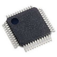
... OXFORD SEMICONDUCTOR LTD ACKAGE NFORMATION OX16C950-PCC60-B OX16C950-TQC60-B Figure 8: 48 Pin Thin Quad Flat Pack (48 TQFP) DS-0031 Sep 05 Figure 7: 44 Pin Plastic Leaded Chip Carrier External—Free Release OX16C950 rev B Page 47 ...
Page 48
... RDERING NFORMATION OX16C950-PCC60-B Revision Operating Conditions -Commercial Package Type - 44 PLCC OX16C950-TQC60-B Revision Package Material - Plastic Package Type - 48 TQFP OX16C950-PLBG RoHS Compliant Revision Package Type - 44 PLCC OX16C950-TQBG RoHS Compliant Revision Package Type – 48 TQFP DS-0031 Sep 05 External—Free Release OX16C950 rev B Page 48 ...
Page 49
... OXFORD SEMICONDUCTOR LTD. N OTES DS-0031 Sep 05 This page has intentionally been left blank. External—Free Release OX16C950 rev B Page 49 ...
Page 50
... Oxford Semiconductor Ltd believes the information contained in this document to be accurate and reliable. However subject to change without notice. No responsibility is assumed by Oxford Semiconductor for its use, nor for infringement of patents or other rights of third parties. No part of this publication may be reproduced, or transmitted in any form or by any means without the ...