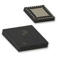
ISP1507BBS ST-Ericsson Inc, ISP1507BBS Datasheet - Page 53

ISP1507BBS
Manufacturer Part Number
ISP1507BBS
Description
IC, TRANSCEIVER, USB OTG, 32HVQFN
Manufacturer
ST-Ericsson Inc
Datasheet
1.ISP1507BBS.pdf
(81 pages)
Specifications of ISP1507BBS
Usb Type
USB Transceiver
Usb Version
2.0
Data Rate
12Mbps
No. Of Ports
1
Supply Voltage Range
3V To 3.6V
Operating Temperature Range
-40°C To +85°C
Digital Ic Case Style
QFN
No. Of Pins
32
Lead Free Status / RoHS Status
Lead free / RoHS Compliant
Available stocks
Company
Part Number
Manufacturer
Quantity
Price
Company:
Part Number:
ISP1507BBSTM
Manufacturer:
SEMIKRON
Quantity:
22
Table 29.
Table 30.
CD00222689
Product data sheet
Bit
Symbol
Reset
Access
Bit
7
6
5
4
3
2
1
0
Symbol
USE_EXT_VBUS_
IND
DRV_VBUS_EXT
DRV_VBUS
CHRG_VBUS
DISCHRG_VBUS
DM_PULLDOWN
DP_PULLDOWN
ID_PULLUP
OTG_CTRL - OTG Control register (address R = 0Ah to 0Ch, W = 0Ah, S = 0Bh, C = 0Ch) bit allocation
OTG_CTRL - OTG Control register (address R = 0Ah to 0Ch, W = 0Ah, S = 0Bh, C = 0Ch) bit
description
USE_EXT_
VBUS_IND
R/W/S/C
7
0
VBUS_EXT
Description
Use External V
0b — Use the internal OTG comparator (default).
1b — Use the external V
Drive V
external charge pump or a 5 V supply is optional.
0b — Drive V
(default).
1b — Drive V
Drive V
then setting DRV_VBUS is optional.
0b — Do not drive V
1b — Drive 5 V on V
Charge V
first check that V
data lines have been LOW (SE0) for 2 ms.
0b — Do not charge V
1b — Charge V
Discharge V
for an RXCMD indicating that SESS_END has changed from 0 to 1, and then resets this bit to
0 to stop the discharge.
0b — Do not discharge V
1b — Discharge V
DM Pull Down: Enables the 15 kΩ pull-down resistor on DM.
0b — Pull-down resistor is not connected to DM.
1b — Pull-down resistor is connected to DM (default).
DP Pull Down: Enables the 15 kΩ pull-down resistor on DP.
0b — Pull-down resistor is not connected to DP.
1b — Pull-down resistor is connected to DP (default).
ID Pull Up: Connects a pull-up to the ID line and enables sampling of the ID level. Disabling
the ID line sampler will reduce PHY power consumption.
0b — Disables sampling of the ID line (default).
1b — Enables sampling of the ID line.
R/W/S/C
DRV_
6
0
BUS
BUS
BUS
: Signals the ISP1507 to drive 5 V on V
External: Selects between the internal and external 5 V V
BUS
BUS
BUS
: Charges V
R/W/S/C
DRV_
VBUS
BUS
BUS
: Discharges V
BUS
using the internal charge pump. Also ensures PSW_N is not driven to LOW
using the external charge pump or the 5 V supply. Drives PSW_N to LOW.
5
0
BUS
.
Indicator: Informs the PHY to use an external V
BUS
BUS
is discharged (see bit DISCHRG_VBUS), and that both the DP and DM
.
Rev. 04 — 20 May 2010
BUS
.
(default).
BUS
BUS
BUS
(default).
R/W/S/C
CHRG_
valid indicator signal input from the FAULT pin.
VBUS
through a resistor. Used for the V
(default).
BUS
4
0
through a resistor. If the link sets this bit to logic 1, it waits
DISCHRG_
R/W/S/C
VBUS
3
0
ISP1507A; ISP1507B
BUS
. If DRV_VBUS_EXT is set to logic 1,
DM_PULL
R/W/S/C
DOWN
ULPI HS USB OTG transceiver
2
1
BUS
pulsing SRP. The link must
BUS
DP_PULL
R/W/S/C
BUS
DOWN
© ST-ERICSSON 2010. All rights reserved.
overcurrent indicator.
1
1
supply. Using an
ID_PULL
R/W/S/C
UP
0
0
53 of 81


