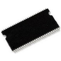
M52S128168A-7.5TG ELITE SEMICONDUCTOR, M52S128168A-7.5TG Datasheet - Page 8

M52S128168A-7.5TG
Manufacturer Part Number
M52S128168A-7.5TG
Description
IC, SDRAM, 128MBIT, 133MHZ, TSOP-54
Manufacturer
ELITE SEMICONDUCTOR
Datasheet
1.M52S128168A-7.5BG.pdf
(47 pages)
Specifications of M52S128168A-7.5TG
Memory Type
DRAM - Sychronous
Memory Configuration
2M X 16
Ic Interface Type
Parallel
Memory Case Style
TSOP
No. Of Pins
54
Operating Temperature Range
0°C To +70°C
Frequency
133MHz
Filter Terminals
SMD
Rohs Compliant
Yes
Page Size
128MB
Lead Free Status / RoHS Status
Lead free / RoHS Compliant
ESMT
SIMPLIFIED TRUTH TABLE
Note :
Elite Semiconductor Memory Technology Inc.
Register
Refresh
Precharge
Clock Suspend or
Active Power Down
Precharge Power Down Mode
DQM
No Operating Command
Column Address
Column Address
Read &
Write &
1.OP Code : Operating Code
2.MRS/EMRS can be issued only at all banks precharge state.
3.Auto refresh functions are as same as CBR refresh of DRAM.
4.BA0~BA1 : Bank select addresses.
5.During burst read or write with auto precharge. new read/write command can not be issued.
6.Burst stop command is valid at every burst length.
7.DQM sampled at positive going edge of a CLK and masks the data-in at the very CLK (write DQM latency is 0), but
Bank Active & Row Addr.
A0~A11 & BA0~BA1 : Program keys. (@ MRS). BA1=0 for MRS and BA1=1 for EMRS
A new command can be issued after 2 CLK cycles of MRS/EMRS.
The automatical precharge without row precharge of command is meant by “Auto”.
Auto/self refresh can be issued only at all banks idle state.
If both BA0 and BA1 are “Low” at read ,write , row active and precharge ,bank A is selected.
If both BA0 is “Low” and BA1 is “High” at read ,write , row active and precharge ,bank B is selected.
If both BA0 is “High” and BA1 is “Low” at read ,write , row active and precharge ,bank C is selected.
If both BA0 and BA1 are “High” at read ,write , row active and precharge ,bank D is selected
If A10/AP is “High” at row precharge , BA0 and BA1 is ignored and all banks are selected.
Another bank read/write command can be issued after the end of burst.
New row active of the associated bank can be issued at tRP after the end of burst.
makes Hi-Z state the data-out of 2 CLK cycles after.(Read DQM latency is 2)
COMMAND
Burst Stop
Mode Register set
Extended Mode Register
set
Auto Refresh
Self
Refresh
Bank Selection
All Banks
Auto Precharge Disable
Auto Precharge Disable
Auto Precharge Enable
Auto Precharge Enable
Entry
Exit
Entry
Entry
Exit
Exit
CKEn-1 CKEn
H
H
H
H
H
H
H
H
H
H
H
L
L
L
(V = Valid , X = Don’t Care. H = Logic High , L = Logic Low )
X
H
H
X
X
X
X
X
H
H
X
L
L
L
CS RAS CAS
H
H
H
H
H
L
L
L
L
L
L
L
L
L
X
L
L
L
H
H
H
H
H
H
X
X
V
X
X
X
V
X
X
L
L
L
L
H
H
H
H
H
H
X
X
V
X
X
X
V
X
L
L
L
L
WE
H
H
H
H
V
H
V
H
X
L
L
L
X
X
X
X
X
L
DQM BA0
Publication Date: Oct. 2007
X
X
X
X
X
X
X
X
X
X
X
X
V
X
X
Revision: 1.1
BA1
V
V
V
V
X
M52S128168A
A10/AP
OP CODE
Row Address
H
H
H
L
L
L
X
X
X
X
X
X
X
Address
(A0~A8)
Column
Column
Address
(A0~A8)
A9~A0
A11
X
8/47
Note
1,2
4,5
4,5
3
3
3
3
4
4
6
7


