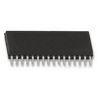
BS62LV1027SIP55 BSI (BRILLIANCE SEMICONDUCTOR), BS62LV1027SIP55 Datasheet - Page 7

BS62LV1027SIP55
Manufacturer Part Number
BS62LV1027SIP55
Description
SRAM 1M, 128KX8, 2.4-5.5V, SOP32
Manufacturer
BSI (BRILLIANCE SEMICONDUCTOR)
Datasheet
1.BS62LV1027SIP55.pdf
(11 pages)
Specifications of BS62LV1027SIP55
Memory Size
1Mbit
Access Time
55ns
Supply Voltage Range
2.4V To 5.5V
Memory Case Style
SOP
No. Of Pins
32
Operating Temperature Range
-40°C To +85°C
Operating Temperature Max
85°C
Operating
RoHS Compliant
Available stocks
Company
Part Number
Manufacturer
Quantity
Price
Company:
Part Number:
BS62LV1027SIP55-TR
Manufacturer:
IDT
Quantity:
101
R0201-BS62LV1027
WRITE CYCLE 2
NOTES:
1. WE must be high during address transitions.
2. The internal write time of the memory is defined by the overlap of CE1 and CE2 active and
3. t
4. During this period, DQ pins are in the output state so that the input signals of opposite
5. If the CE1 low transition or the CE2 high transition occurs simultaneously with the WE low
6. OE is continuously low (OE = V
7. D
8. D
9. If CE1 is low and CE2 is high during this period, DQ pins are in the output state. Then the
10. Transition is measured ± 500mV from steady state with C
11. t
WE low. All signals must be active to initiate a write and any one signal can terminate a
write by going inactive. The data input setup and hold timing should be referenced to the
second transition edge of the signal that terminates the write.
write cycle.
phase to the outputs must not be applied.
transitions or after the WE transition, output remain in a high impedance state.
data input signals of opposite phase to the outputs must not be applied to them.
The parameter is guaranteed but not 100% tested.
WR
CW
OUT
OUT
ADDRESS
CE1
CE2
WE
D
D
is measured from the later of CE1 going low or CE2 going high to the end of write.
is measured from the earlier of CE1 or WE going high or CE2 going low at the end of
is the same phase of write data of this write cycle.
is the read data of next address.
OUT
IN
(1,6)
IL
).
t
AS
(5)
(5)
t
L
WHZ
= 5pF.
(4,10)
7
t
AW
t
t
t
CW
CW
WP
t
WC
(11)
(11)
(2)
t
DW
t
WR2
t
t
OW
DH
(3)
(8,9)
BS62LV1027
(7)
Revision
May.
(8)
2006
2.3


