PIC24FJ256GA106-I/MR Microchip Technology, PIC24FJ256GA106-I/MR Datasheet - Page 146
PIC24FJ256GA106-I/MR
Manufacturer Part Number
PIC24FJ256GA106-I/MR
Description
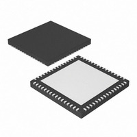
IC, 16BIT MCU, PIC24F, 32MHZ, QFN-64
Manufacturer
Microchip Technology
Series
PIC® 24Fr
Datasheets
1.PIC24FJ128GA008-IPT.pdf
(12 pages)
2.PIC24FJ128GA106-IPT.pdf
(14 pages)
3.PIC24FJ128GA106-IPT.pdf
(330 pages)
4.PIC24FJ128GA106-IPT.pdf
(52 pages)
5.PIC24FJ256GA106-IPT.pdf
(59 pages)
6.PIC24FJ128GB110-IPF.pdf
(292 pages)
Specifications of PIC24FJ256GA106-I/MR
Controller Family/series
PIC24
No. Of I/o's
53
Ram Memory Size
16KB
Cpu Speed
32MHz
No. Of Timers
5
Core Size
16 Bit
Program Memory Size
256KB
Peripherals
ADC, Comparator, PWM, RTC, Timer
Core Processor
PIC
Speed
32MHz
Connectivity
I²C, PMP, SPI, UART/USART
Number Of I /o
53
Program Memory Type
FLASH
Ram Size
16K x 8
Voltage - Supply (vcc/vdd)
2 V ~ 3.6 V
Data Converters
A/D 16x10b
Oscillator Type
Internal
Operating Temperature
-40°C ~ 85°C
Package / Case
64-VFQFN, Exposed Pad
Processor Series
PIC24FJ
Core
PIC
Data Bus Width
16 bit
Data Ram Size
16 KB
Interface Type
I2C, SPI, UART
Maximum Clock Frequency
32 MHz
Number Of Programmable I/os
52
Number Of Timers
5
Maximum Operating Temperature
+ 85 C
Mounting Style
SMD/SMT
3rd Party Development Tools
52713-733, 52714-737, 53276-922, EWDSPIC
Development Tools By Supplier
PG164130, DV164035, DV244005, DV164005, PG164120, DM240001, DM240011
Minimum Operating Temperature
- 40 C
On-chip Adc
10 bit, 16 Channel
Lead Free Status / RoHS Status
Lead free / RoHS Compliant
For Use With
876-1004 - PIC24 BREAKOUT BOARD
Eeprom Size
-
Lead Free Status / Rohs Status
Details


PIC24FJ256GA110 FAMILY
REGISTER 10-22: RPOR0: PERIPHERAL PIN SELECT OUTPUT REGISTER 0
REGISTER 10-23: RPOR1: PERIPHERAL PIN SELECT OUTPUT REGISTER 1
DS39905E-page 146
bit 15
bit 7
Legend:
R = Readable bit
-n = Value at POR
bit 15-14
bit 13-8
bit 7-6
bit 5-0
bit 15
bit 7
Legend:
R = Readable bit
-n = Value at POR
bit 15-14
bit 13-8
bit 7-6
bit 5-0
U-0
U-0
U-0
U-0
—
—
—
—
Unimplemented: Read as ‘0’
RP1R<5:0>: RP1 Output Pin Mapping bits
Peripheral output number n is assigned to pin, RP1 (see
Unimplemented: Read as ‘0’
RP0R<5:0>: RP0 Output Pin Mapping bits
Peripheral output number n is assigned to pin, RP0 (see
Unimplemented: Read as ‘0’
RP3R<5:0>: RP3 Output Pin Mapping bits
Peripheral output number n is assigned to pin, RP3 (see
Unimplemented: Read as ‘0’
RP2R<5:0>: RP2 Output Pin Mapping bits
Peripheral output number n is assigned to pin, RP2 (see
U-0
U-0
U-0
U-0
—
—
—
—
W = Writable bit
‘1’ = Bit is set
W = Writable bit
‘1’ = Bit is set
RP1R5
RP0R5
RP3R5
RP2R5
R/W-0
R/W-0
R/W-0
R/W-0
RP1R4
RP0R4
RP3R4
RP2R4
R/W-0
R/W-0
R/W-0
R/W-0
U = Unimplemented bit, read as ‘0’
‘0’ = Bit is cleared
U = Unimplemented bit, read as ‘0’
‘0’ = Bit is cleared
RP1R3
RP0R3
RP3R3
RP2R3
R/W-0
R/W-0
R/W-0
R/W-0
Table 10-3
Table 10-3
Table 10-3
Table 10-3
RP1R2
RP0R2
RP3R2
RP2R2
R/W-0
R/W-0
R/W-0
R/W-0
for peripheral function numbers).
for peripheral function numbers).
for peripheral function numbers).
for peripheral function numbers).
2010 Microchip Technology Inc.
x = Bit is unknown
x = Bit is unknown
RP1R1
RP0R1
RP3R1
RP2R1
R/W-0
R/W-0
R/W-0
R/W-0
RP1R0
RP0R0
RP3R0
RP2R0
R/W-0
R/W-0
R/W-0
R/W-0
bit 8
bit 0
bit 8
bit 0
Related parts for PIC24FJ256GA106-I/MR
Image
Part Number
Description
Manufacturer
Datasheet
Request
R

Part Number:
Description:
Manufacturer:
Microchip Technology Inc.
Datasheet:
Part Number:
Description:
Manufacturer:
Microchip Technology Inc.
Datasheet:
Part Number:
Description:
Manufacturer:
Microchip Technology Inc.
Datasheet:
Part Number:
Description:
Manufacturer:
Microchip Technology Inc.
Datasheet:
Part Number:
Description:
Manufacturer:
Microchip Technology Inc.
Datasheet:
Part Number:
Description:
Manufacturer:
Microchip Technology Inc.
Datasheet:
Part Number:
Description:
Manufacturer:
Microchip Technology Inc.
Datasheet:
Part Number:
Description:
Manufacturer:
Microchip Technology Inc.
Datasheet: