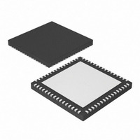
PIC24FJ256GA106-I/MR Microchip Technology, PIC24FJ256GA106-I/MR Datasheet - Page 163

PIC24FJ256GA106-I/MR
Manufacturer Part Number
PIC24FJ256GA106-I/MR
Description
IC, 16BIT MCU, PIC24F, 32MHZ, QFN-64
Manufacturer
Microchip Technology
Series
PIC® 24Fr
Datasheets
1.PIC24FJ128GA008-IPT.pdf
(12 pages)
2.PIC24FJ128GA106-IPT.pdf
(14 pages)
3.PIC24FJ128GA106-IPT.pdf
(330 pages)
4.PIC24FJ128GA106-IPT.pdf
(52 pages)
5.PIC24FJ256GA106-IPT.pdf
(59 pages)
6.PIC24FJ128GB110-IPF.pdf
(292 pages)
Specifications of PIC24FJ256GA106-I/MR
Controller Family/series
PIC24
No. Of I/o's
53
Ram Memory Size
16KB
Cpu Speed
32MHz
No. Of Timers
5
Core Size
16 Bit
Program Memory Size
256KB
Peripherals
ADC, Comparator, PWM, RTC, Timer
Core Processor
PIC
Speed
32MHz
Connectivity
I²C, PMP, SPI, UART/USART
Number Of I /o
53
Program Memory Type
FLASH
Ram Size
16K x 8
Voltage - Supply (vcc/vdd)
2 V ~ 3.6 V
Data Converters
A/D 16x10b
Oscillator Type
Internal
Operating Temperature
-40°C ~ 85°C
Package / Case
64-VFQFN, Exposed Pad
Processor Series
PIC24FJ
Core
PIC
Data Bus Width
16 bit
Data Ram Size
16 KB
Interface Type
I2C, SPI, UART
Maximum Clock Frequency
32 MHz
Number Of Programmable I/os
52
Number Of Timers
5
Maximum Operating Temperature
+ 85 C
Mounting Style
SMD/SMT
3rd Party Development Tools
52713-733, 52714-737, 53276-922, EWDSPIC
Development Tools By Supplier
PG164130, DV164035, DV244005, DV164005, PG164120, DM240001, DM240011
Minimum Operating Temperature
- 40 C
On-chip Adc
10 bit, 16 Channel
Lead Free Status / RoHS Status
Lead free / RoHS Compliant
For Use With
876-1004 - PIC24 BREAKOUT BOARD
Eeprom Size
-
Lead Free Status / Rohs Status
Details
- PIC24FJ128GA008-IPT PDF datasheet
- PIC24FJ128GA106-IPT PDF datasheet #2
- PIC24FJ128GA106-IPT PDF datasheet #3
- PIC24FJ128GA106-IPT PDF datasheet #4
- PIC24FJ256GA106-IPT PDF datasheet #5
- PIC24FJ128GB110-IPF PDF datasheet #6
- Current page: 163 of 330
- Download datasheet (3Mb)
13.0
Devices in the PIC24FJ256GA110 family all feature
9 independent enhanced input capture modules. Each
of the modules offers a wide range of configuration and
operating options for capturing external pulse events
and generating interrupts.
Key features of the enhanced output module include:
• Hardware-configurable for 32-bit operation in all
• Synchronous and Trigger modes of output
• A 4-level FIFO buffer for capturing and holding
• Configurable interrupt generation
• Up to 6 clock sources available for each module,
The module is controlled through two registers: ICxCON1
(Register
block diagram of the module is shown in
FIGURE 13-1:
2010 Microchip Technology Inc.
Note:
modes by cascading two adjacent modules
compare operation, with up to 30 user-selectable
trigger/sync sources available
timer values for several events
driving a separate internal 16-bit counter
Trigger and
Sync Sources
IC Clock
Sources
Note 1: The ICx inputs must be assigned to an available RPn pin before use. Please see
ICx Pin
INPUT CAPTURE WITH
DEDICATED TIMER
13-1) and ICxCON2
Section
Dedicated Timer” (DS39722)
This data sheet summarizes the features of
this group of PIC24F devices. It is not
intended to be a comprehensive reference
source. For more information, refer to the
“PIC24F
(1)
Pin Select”
ICTSEL<2:0>
Trigger and
Sync Logic
Prescaler
34.
Family
INPUT CAPTURE BLOCK DIAGRAM
Counter
1:1/4/16
Select
Clock
for more information.
“Input
(Register
Reference
Increment
Reset
Capture
13-2). A general
ICM<2:0>
Figure
SYNCSEL<4:0>
TRIGGER
Clock Synchronizer
Edge Detect Logic
Manual”,
13-1.
PIC24FJ256GA110 FAMILY
ICxTMR
and
with
13.1
13.1.1
By default, the enhanced input capture module oper-
ates in a free-running mode. The internal 16-bit counter
ICxTMR counts up continuously, wrapping around from
FFFFh to 0000h on each overflow, with its period
synchronized to the selected external clock source.
When a capture event occurs, the current 16-bit value
of the internal counter is written to the FIFO buffer.
In Synchronous mode, the module begins capturing
events on the ICx pin as soon as its selected clock
source is enabled. Whenever an event occurs on the
selected sync source, the internal counter is reset. In
Trigger mode, the module waits for a Sync event from
another internal module to occur before allowing the
internal counter to run.
Standard, free-running operation is selected by setting
the SYNCSEL bits to ‘00000’ and clearing the ICTRIG
bit (ICxCON2<7>). Synchronous and Trigger modes
are selected any time the SYNCSEL bits are set to any
value except ‘00000’. The ICTRIG bit selects either
Synchronous or Trigger mode; setting the bit selects
Trigger mode operation. In both modes, the SYNCSEL
bits determine the sync/trigger source.
When the SYNCSEL bits are set to ‘00000’ and
ICTRIG is set, the module operates in Software Trigger
mode. In this case, capture operations are started by
manually setting the TRIGSTAT bit (ICxCON2<6>).
16
General Operating Modes
SYNCHRONOUS AND TRIGGER
MODES
4-Level FIFO Buffer
ICOV, ICBNE
ICI<1:0>
Event and
Interrupt
ICxBUF
Logic
(1)
Section 10.4 “Peripheral
Set ICxIF
DS39905E-page 163
16
System Bus
16
Related parts for PIC24FJ256GA106-I/MR
Image
Part Number
Description
Manufacturer
Datasheet
Request
R

Part Number:
Description:
Manufacturer:
Microchip Technology Inc.
Datasheet:

Part Number:
Description:
Manufacturer:
Microchip Technology Inc.
Datasheet:

Part Number:
Description:
Manufacturer:
Microchip Technology Inc.
Datasheet:

Part Number:
Description:
Manufacturer:
Microchip Technology Inc.
Datasheet:

Part Number:
Description:
Manufacturer:
Microchip Technology Inc.
Datasheet:

Part Number:
Description:
Manufacturer:
Microchip Technology Inc.
Datasheet:

Part Number:
Description:
Manufacturer:
Microchip Technology Inc.
Datasheet:

Part Number:
Description:
Manufacturer:
Microchip Technology Inc.
Datasheet:


