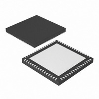
PIC24FJ256GA106-I/MR Microchip Technology, PIC24FJ256GA106-I/MR Datasheet - Page 170

PIC24FJ256GA106-I/MR
Manufacturer Part Number
PIC24FJ256GA106-I/MR
Description
IC, 16BIT MCU, PIC24F, 32MHZ, QFN-64
Manufacturer
Microchip Technology
Series
PIC® 24Fr
Datasheets
1.PIC24FJ128GA008-IPT.pdf
(12 pages)
2.PIC24FJ128GA106-IPT.pdf
(14 pages)
3.PIC24FJ128GA106-IPT.pdf
(330 pages)
4.PIC24FJ128GA106-IPT.pdf
(52 pages)
5.PIC24FJ256GA106-IPT.pdf
(59 pages)
6.PIC24FJ128GB110-IPF.pdf
(292 pages)
Specifications of PIC24FJ256GA106-I/MR
Controller Family/series
PIC24
No. Of I/o's
53
Ram Memory Size
16KB
Cpu Speed
32MHz
No. Of Timers
5
Core Size
16 Bit
Program Memory Size
256KB
Peripherals
ADC, Comparator, PWM, RTC, Timer
Core Processor
PIC
Speed
32MHz
Connectivity
I²C, PMP, SPI, UART/USART
Number Of I /o
53
Program Memory Type
FLASH
Ram Size
16K x 8
Voltage - Supply (vcc/vdd)
2 V ~ 3.6 V
Data Converters
A/D 16x10b
Oscillator Type
Internal
Operating Temperature
-40°C ~ 85°C
Package / Case
64-VFQFN, Exposed Pad
Processor Series
PIC24FJ
Core
PIC
Data Bus Width
16 bit
Data Ram Size
16 KB
Interface Type
I2C, SPI, UART
Maximum Clock Frequency
32 MHz
Number Of Programmable I/os
52
Number Of Timers
5
Maximum Operating Temperature
+ 85 C
Mounting Style
SMD/SMT
3rd Party Development Tools
52713-733, 52714-737, 53276-922, EWDSPIC
Development Tools By Supplier
PG164130, DV164035, DV244005, DV164005, PG164120, DM240001, DM240011
Minimum Operating Temperature
- 40 C
On-chip Adc
10 bit, 16 Channel
Lead Free Status / RoHS Status
Lead free / RoHS Compliant
For Use With
876-1004 - PIC24 BREAKOUT BOARD
Eeprom Size
-
Lead Free Status / Rohs Status
Details
- PIC24FJ128GA008-IPT PDF datasheet
- PIC24FJ128GA106-IPT PDF datasheet #2
- PIC24FJ128GA106-IPT PDF datasheet #3
- PIC24FJ128GA106-IPT PDF datasheet #4
- PIC24FJ256GA106-IPT PDF datasheet #5
- PIC24FJ128GB110-IPF PDF datasheet #6
- Current page: 170 of 330
- Download datasheet (3Mb)
PIC24FJ256GA110 FAMILY
FIGURE 14-2:
14.3.1
The PWM period is specified by writing to PRy, the
Timer Period register. The PWM period can be
calculated using
EQUATION 14-1:
DS39905E-page 170
PWM Period = [(PRy) + 1] • T
where:
Note 1:
Note:
Trigger and
Sync Sources
OC Clock
Sources
Note 1: The OCx outputs must be assigned to an available RPn pin before use. Please see
PWM Frequency = 1/[PWM Period]
PWM PERIOD
A PRy value of N will produce a PWM
period of N + 1 time base count cycles. For
example, a value of 7 written into the PRy
register will yield a period consisting of
8 time base cycles.
Based on T
and PLL are disabled.
TRIGMODE
SYNCSELx
TRIGSTAT
Pin Select”
OCTSELx
Equation
OCTRIG
Trigger and
Sync Logic
OUTPUT COMPARE BLOCK DIAGRAM (DOUBLE-BUFFERED, 16-BIT PWM MODE)
CALCULATING THE PWM
PERIOD
CY
Clock
Select
14-1.
= T
for more information.
Reset
CY
OSC
• (Timer Prescale Value)
(1)
* 2, Doze mode
Match Event
Increment
Reset
OCxRS buffer
OCxR Buffer
Comparator
Comparator
OCxCON1
OCxCON2
OCxTMR
OCxRS
OCxR
Rollover/Reset
Rollover/Reset
14.3.2
The PWM duty cycle is specified by writing to the
OCxRS and OCxR registers. The OCxRS and OCxR
registers can be written to at any time, but the duty
cycle value is not latched until a match between PRy
and TMRy occurs (i.e., the period is complete). This
provides a double buffer for the PWM duty cycle and is
essential for glitchless PWM operation.
Some important boundary parameters of the PWM duty
cycle include:
• If OCxR, OCxRS and PRy are all loaded with
• ·If OCxRS is greater than PRy, the pin will remain
See
Table 14-1
frequencies and resolutions for a device operating at
4 MIPS and 10 MIPS, respectively.
Match
Event
Match
Event
Rollover
0000h, the OCx pin will remain low (0% duty
cycle).
high (100% duty cycle).
Example 14-1
PWM DUTY CYCLE
and
OC Output and
Fault Logic
Table 14-2
OCx Interrupt
for PWM mode timing details.
OCMx
OCINV
OCTRIS
FLTOUT
FLTTRIEN
FLTMD
ENFLT0
OCFLT0
2010 Microchip Technology Inc.
(1)
Section 10.4 “Peripheral
show example PWM
OCFA/OCFB
OCx Pin
Related parts for PIC24FJ256GA106-I/MR
Image
Part Number
Description
Manufacturer
Datasheet
Request
R

Part Number:
Description:
Manufacturer:
Microchip Technology Inc.
Datasheet:

Part Number:
Description:
Manufacturer:
Microchip Technology Inc.
Datasheet:

Part Number:
Description:
Manufacturer:
Microchip Technology Inc.
Datasheet:

Part Number:
Description:
Manufacturer:
Microchip Technology Inc.
Datasheet:

Part Number:
Description:
Manufacturer:
Microchip Technology Inc.
Datasheet:

Part Number:
Description:
Manufacturer:
Microchip Technology Inc.
Datasheet:

Part Number:
Description:
Manufacturer:
Microchip Technology Inc.
Datasheet:

Part Number:
Description:
Manufacturer:
Microchip Technology Inc.
Datasheet:


