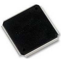
LPC2220FBD144 NXP Semiconductors, LPC2220FBD144 Datasheet - Page 18

LPC2220FBD144
Manufacturer Part Number
LPC2220FBD144
Description
IC, 16/32BIT ARM7 MCU, 64K RAM, SMD
Manufacturer
NXP Semiconductors
Datasheet
1.LPC2220FBD144.pdf
(50 pages)
Specifications of LPC2220FBD144
No. Of I/o's
76
Ram Memory Size
64KB
Cpu Speed
75MHz
No. Of Timers
2
No. Of Pwm Channels
6
Digital Ic Case Style
LQFP
Supply Voltage
RoHS Compliant
Core Size
32bit
Oscillator Type
External Only
Controller Family/series
LPC22xx
Peripherals
ADC, RTC
Rohs Compliant
Yes
Available stocks
Company
Part Number
Manufacturer
Quantity
Price
Company:
Part Number:
LPC2220FBD144
Manufacturer:
NXP
Quantity:
5 000
Company:
Part Number:
LPC2220FBD144
Manufacturer:
NXP
Quantity:
530
Part Number:
LPC2220FBD144
Manufacturer:
NXP/恩智浦
Quantity:
20 000
Company:
Part Number:
LPC2220FBD144,551
Manufacturer:
Microchip
Quantity:
150
Company:
Part Number:
LPC2220FBD144,551
Manufacturer:
NXP Semiconductors
Quantity:
10 000
Part Number:
LPC2220FBD144,551
Manufacturer:
NXP/恩智浦
Quantity:
20 000
Company:
Part Number:
LPC2220FBD144/01
Manufacturer:
FSC
Quantity:
30
NXP Semiconductors
LPC2210_2220_6
Product data sheet
6.5 Pin connect block
6.6 Pin function select register 0 (PINSEL0 - 0xE002 C000)
The pin connect block allows selected pins of the microcontroller to have more than one
function. Configuration registers control the multiplexers to allow connection between the
pin and the on chip peripherals. Peripherals should be connected to the appropriate pins
prior to being activated, and prior to any related interrupt(s) being enabled. Activity of any
enabled peripheral function that is not mapped to a related pin should be considered
undefined.
The pin control module contains three registers as shown in
Table 6.
The PINSEL0 register controls the functions of the pins as per the settings listed in
Table
function is selected for a pin. For other functions, direction is controlled automatically.
Settings other than those shown in
Table 7.
Address
0xE002 C000
0xE002 C004
0xE002 C014
PINSEL0
1:0
3:2
5:4
7:6
9:8
7. The direction control bit in the IODIR register is effective only when the GPIO
Pin control module registers
Pin function select register 0 (PINSEL0 - 0xE002 C000)
Pin name
P0.0
P0.1
P0.2
P0.3
P0.4
Name
PINSEL0
PINSEL1
PINSEL2
Rev. 06 — 11 December 2008
Value
0
0
1
1
0
0
1
1
0
0
1
1
0
0
1
1
0
0
1
1
0
1
0
1
0
1
0
1
0
1
0
1
0
1
0
1
0
1
0
1
Table 7
Description
pin function select register 0
pin function select register 1
pin function select register 2
are reserved, and should not be used
Function
GPIO Port 0.0
TXD0 (UART0)
PWM1
reserved
GPIO Port 0.1
RXD0 (UART0)
PWM3
EINT0
GPIO Port 0.2
SCL (I
Capture 0.0 (Timer 0)
reserved
GPIO Port 0.3
SDA (I
Match 0.0 (Timer 0)
EINT1
GPIO Port 0.4
SCK (SPI0)
Capture 0.1 (Timer 0)
reserved
2
2
C-bus)
C-bus)
16/32-bit ARM microcontrollers
LPC2210/2220
Table
6.
Value after reset
0
0
0
0
0
© NXP B.V. 2008. All rights reserved.
Access
read/write
read/write
read/write
18 of 50


