PIC24FJ256GB106-I/MR Microchip Technology, PIC24FJ256GB106-I/MR Datasheet - Page 294
PIC24FJ256GB106-I/MR
Manufacturer Part Number
PIC24FJ256GB106-I/MR
Description
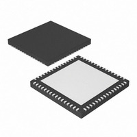
IC, 16BIT MCU, PIC24F, 32MHZ, QFN-64
Manufacturer
Microchip Technology
Series
PIC® 24Fr
Datasheets
1.PIC24FJ128GA106-IPT.pdf
(52 pages)
2.PIC24FJ64GB106-IPT.pdf
(16 pages)
3.PIC24FJ64GB106-IPT.pdf
(352 pages)
4.PIC24FJ192GB108-IPT.pdf
(328 pages)
Specifications of PIC24FJ256GB106-I/MR
Controller Family/series
PIC24
No. Of I/o's
51
Ram Memory Size
16KB
Cpu Speed
32MHz
No. Of Timers
5
Core Size
16 Bit
Program Memory Size
256KB
Peripherals
ADC, Comparator, PWM, RTC, Timer
Core Processor
PIC
Speed
32MHz
Connectivity
I²C, SPI, UART/USART, USB OTG
Number Of I /o
51
Program Memory Type
FLASH
Ram Size
16K x 8
Voltage - Supply (vcc/vdd)
2 V ~ 3.6 V
Data Converters
A/D 16x10b
Oscillator Type
Internal
Operating Temperature
-40°C ~ 85°C
Package / Case
64-VFQFN, Exposed Pad
Processor Series
PIC24FJ
Core
PIC
Data Bus Width
16 bit
Data Ram Size
16 KB
Interface Type
I2C, SPI, UART
Maximum Clock Frequency
32 MHz
Number Of Programmable I/os
52
Number Of Timers
5
Maximum Operating Temperature
+ 85 C
Mounting Style
SMD/SMT
3rd Party Development Tools
52713-733, 52714-737, 53276-922, EWDSPIC
Development Tools By Supplier
PG164130, DV164035, DV244005, DV164005, PG164120, DM240001, DM240011
Minimum Operating Temperature
- 40 C
On-chip Adc
10 bit, 16 Channel
Lead Free Status / RoHS Status
Lead free / RoHS Compliant
For Use With
876-1004 - PIC24 BREAKOUT BOARD
Eeprom Size
-
Lead Free Status / Rohs Status
Details
Available stocks
Company
Part Number
Manufacturer
Quantity
Price
Company:

Part Number:
PIC24FJ256GB106-I/MR
Manufacturer:
TI
Quantity:
1 292


PIC24FJ256GB110 FAMILY
26.2.2
When the voltage regulator is enabled, it takes approxi-
mately 10 s for it to generate output. During this time,
designated as T
is applied every time the device resumes operation after
any power-down, including Sleep mode. The length of
T
described in Section 26.2.5 “Voltage Regulator
Standby Mode”.
If the regulator is disabled, a separate Power-up Timer
(PWRT) is automatically enabled. The PWRT adds a
fixed delay of 64 ms nominal delay at device start-up
(POR or BOR only). When waking up from Sleep with
the regulator disabled, the PMSLP bit determines the
wake-up time. When operating with the regulator
disabled, setting PMSLP can decrease the device
wake-up time.
26.2.3
When
PIC24FJ256GB110 family devices also have a simple
brown-out capability. If the voltage supplied to the reg-
ulator is inadequate to maintain the tracking level, the
regulator Reset circuitry will generate a Brown-out
Reset. This event is captured by the BOR flag bit
(RCON<1>). The brown-out voltage specifications are
provided in the “PIC24FJ Family Reference Manual”,
Section 7. “Reset” (DS39712).
26.2.4
The on-chip regulator is designed to meet the power-up
requirements for the device. If the application does not
use the regulator, then strict power-up conditions must
be adhered to. While powering up, V
never exceed V
26.2.5
When enabled, the on-chip regulator always consumes
a small incremental amount of current over I
including when the device is in Sleep mode, even
though the core digital logic does not require power. To
provide additional savings in applications where power
resources are critical, the regulator automatically
disables itself whenever the device goes into Sleep
mode. This feature is controlled by the PMSLP bit
(RCON<8>). By default, the bit is cleared, which
removes power from the Flash program memory and
thus enables Standby mode. When waking up from
Standby mode, the regulator must wait for T
expire before wake-up. This extra time is needed to
ensure that the regulator can source enough current to
power the Flash memory.
DS39897C-page 294
VREG
Note:
is determined by the PMSLP bit (RCON<8>), as
the
ON-CHIP REGULATOR AND POR
ON-CHIP REGULATOR AND BOR
POWER-UP REQUIREMENTS
For more information, see Section 29.0
“Electrical Characteristics”.
VOLTAGE REGULATOR STANDBY
MODE
VREG
DD
on-chip
by 0.3 volts.
, code execution is disabled. T
regulator
is
DDCORE
enabled,
VREG
DD
VREG
must
/I
PD
to
,
For applications which require a faster wake-up time, it
is possible to disable regulator Standby mode. The
PMSLP bit can be set to turn off Standby mode so that
the Flash stays powered when in Sleep mode and the
device can wake-up without waiting for T
PMSLP is set, the power consumption while in Sleep
mode, will be approximately 40 A higher than power
consumption when the regulator is allowed to enter
Standby mode.
26.3
For PIC24FJ256GB110 family devices, the WDT is
driven by the LPRC Oscillator. When the WDT is
enabled, the clock source is also enabled.
The nominal WDT clock source from LPRC is 31 kHz.
This feeds a prescaler that can be configured for either
5-bit (divide-by-32) or 7-bit (divide-by-128) operation.
The prescaler is set by the FWPSA Configuration bit.
With a 31 kHz input, the prescaler yields a nominal
WDT time-out period (T
4 ms in 7-bit mode.
A variable postscaler divides down the WDT prescaler
output and allows for a wide range of time-out periods.
The postscaler is controlled by the WDTPS<3:0> Con-
figuration bits (CW1<3:0>), which allow the selection of
a total of 16 settings, from 1:1 to 1:32,768. Using the
prescaler and postscaler, time-out periods ranging from
1 ms to 131 seconds can be achieved.
The WDT, prescaler and postscaler are reset:
• On any device Reset
• On the completion of a clock switch, whether
• When a PWRSAV instruction is executed
• When the device exits Sleep or Idle mode to
• By a CLRWDT instruction during normal execution
If the WDT is enabled, it will continue to run during
Sleep or Idle modes. When the WDT time-out occurs,
the device will wake the device and code execution will
continue from where the PWRSAV instruction was exe-
cuted. The corresponding SLEEP or IDLE bits
(RCON<3:2>) will need to be cleared in software after
the device wakes up.
The WDT Flag bit, WDTO (RCON<4>), is not auto-
matically cleared following a WDT time-out. To detect
subsequent WDT events, the flag must be cleared in
software.
invoked by software (i.e., setting the OSWEN bit
after changing the NOSC bits) or by hardware
(i.e., Fail-Safe Clock Monitor)
(i.e., Sleep or Idle mode is entered)
resume normal operation
Note:
Watchdog Timer (WDT)
The CLRWDT and PWRSAV instructions
clear the prescaler and postscaler counts
when executed.
2009 Microchip Technology Inc.
WDT
) of 1 ms in 5-bit mode, or
VREG
. When
Related parts for PIC24FJ256GB106-I/MR
Image
Part Number
Description
Manufacturer
Datasheet
Request
R

Part Number:
Description:
Manufacturer:
Microchip Technology Inc.
Datasheet:
Part Number:
Description:
Manufacturer:
Microchip Technology Inc.
Datasheet:
Part Number:
Description:
Manufacturer:
Microchip Technology Inc.
Datasheet:
Part Number:
Description:
Manufacturer:
Microchip Technology Inc.
Datasheet:
Part Number:
Description:
Manufacturer:
Microchip Technology Inc.
Datasheet:
Part Number:
Description:
Manufacturer:
Microchip Technology Inc.
Datasheet:
Part Number:
Description:
Manufacturer:
Microchip Technology Inc.
Datasheet:
Part Number:
Description:
Manufacturer:
Microchip Technology Inc.
Datasheet: