PIC24FJ256GB106-I/MR Microchip Technology, PIC24FJ256GB106-I/MR Datasheet - Page 41
PIC24FJ256GB106-I/MR
Manufacturer Part Number
PIC24FJ256GB106-I/MR
Description
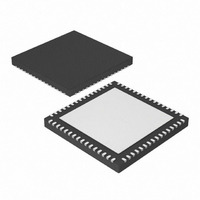
IC, 16BIT MCU, PIC24F, 32MHZ, QFN-64
Manufacturer
Microchip Technology
Series
PIC® 24Fr
Datasheets
1.PIC24FJ128GA106-IPT.pdf
(52 pages)
2.PIC24FJ64GB106-IPT.pdf
(16 pages)
3.PIC24FJ64GB106-IPT.pdf
(352 pages)
4.PIC24FJ192GB108-IPT.pdf
(328 pages)
Specifications of PIC24FJ256GB106-I/MR
Controller Family/series
PIC24
No. Of I/o's
51
Ram Memory Size
16KB
Cpu Speed
32MHz
No. Of Timers
5
Core Size
16 Bit
Program Memory Size
256KB
Peripherals
ADC, Comparator, PWM, RTC, Timer
Core Processor
PIC
Speed
32MHz
Connectivity
I²C, SPI, UART/USART, USB OTG
Number Of I /o
51
Program Memory Type
FLASH
Ram Size
16K x 8
Voltage - Supply (vcc/vdd)
2 V ~ 3.6 V
Data Converters
A/D 16x10b
Oscillator Type
Internal
Operating Temperature
-40°C ~ 85°C
Package / Case
64-VFQFN, Exposed Pad
Processor Series
PIC24FJ
Core
PIC
Data Bus Width
16 bit
Data Ram Size
16 KB
Interface Type
I2C, SPI, UART
Maximum Clock Frequency
32 MHz
Number Of Programmable I/os
52
Number Of Timers
5
Maximum Operating Temperature
+ 85 C
Mounting Style
SMD/SMT
3rd Party Development Tools
52713-733, 52714-737, 53276-922, EWDSPIC
Development Tools By Supplier
PG164130, DV164035, DV244005, DV164005, PG164120, DM240001, DM240011
Minimum Operating Temperature
- 40 C
On-chip Adc
10 bit, 16 Channel
Lead Free Status / RoHS Status
Lead free / RoHS Compliant
For Use With
876-1004 - PIC24 BREAKOUT BOARD
Eeprom Size
-
Lead Free Status / Rohs Status
Details
Available stocks
Company
Part Number
Manufacturer
Quantity
Price
Company:

Part Number:
PIC24FJ256GB106-I/MR
Manufacturer:
TI
Quantity:
1 292


4.2
The PIC24F core has a separate, 16-bit wide data mem-
ory space, addressable as a single linear range. The
data space is accessed using two Address Generation
Units (AGUs), one each for read and write operations.
The data space memory map is shown in Figure 4-3.
All Effective Addresses (EAs) in the data memory space
are 16 bits wide and point to bytes within the data space.
This gives a data space address range of 64 Kbytes or
32K words. The lower half of the data memory space
(that is, when EA<15> = 0) is used for implemented
memory addresses, while the upper half (EA<15> = 1) is
reserved for the program space visibility area (see
Section 4.3.3 “Reading Data from Program Memory
Using Program Space Visibility”).
FIGURE 4-3:
2009 Microchip Technology Inc.
Note:
Data Address Space
Implemented
Data RAM
Data memory areas are not shown to scale.
DATA SPACE MEMORY MAP FOR PIC24FJ256GB110 FAMILY DEVICES
Address
FFFFh
1FFFh
7FFFh
07FFh
47FFh
0001h
0801h
2001h
4801h
8001h
MSB
MSB
PIC24FJ256GB110 FAMILY
Unimplemented
Program Space
Visibility Area
SFR Space
Read as ‘0’
Data RAM
LSB
PIC24FJ256GB110 family devices implement a total of
16 Kbytes of data memory. Should an EA point to a
location outside of this area, an all zero word or byte will
be returned.
4.2.1
The
byte-addressable, 16-bit wide blocks. Data is aligned
in data memory and registers as 16-bit words, but all
data space EAs resolve to bytes. The Least Significant
Bytes of each word have even addresses, while the
Most Significant Bytes have odd addresses.
data
DATA SPACE WIDTH
Address
0000h
07FEh
0800h
1FFEh
2000h
47FEh
4800h
7FFFh
8000h
FFFEh
LSB
memory
Space
SFR
space
Data Space
is
DS39897C-page 41
Near
organized
in
Related parts for PIC24FJ256GB106-I/MR
Image
Part Number
Description
Manufacturer
Datasheet
Request
R

Part Number:
Description:
Manufacturer:
Microchip Technology Inc.
Datasheet:
Part Number:
Description:
Manufacturer:
Microchip Technology Inc.
Datasheet:
Part Number:
Description:
Manufacturer:
Microchip Technology Inc.
Datasheet:
Part Number:
Description:
Manufacturer:
Microchip Technology Inc.
Datasheet:
Part Number:
Description:
Manufacturer:
Microchip Technology Inc.
Datasheet:
Part Number:
Description:
Manufacturer:
Microchip Technology Inc.
Datasheet:
Part Number:
Description:
Manufacturer:
Microchip Technology Inc.
Datasheet:
Part Number:
Description:
Manufacturer:
Microchip Technology Inc.
Datasheet: