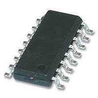
TEA1751LT/N1 NXP Semiconductors, TEA1751LT/N1 Datasheet - Page 10

TEA1751LT/N1
Manufacturer Part Number
TEA1751LT/N1
Description
AC-DC, PFC, FLYBACK, CNTRL, 16SOIC
Manufacturer
NXP Semiconductors
Datasheet
1.TEA1751LTN1518.pdf
(29 pages)
Specifications of TEA1751LT/N1
Input Voltage
276V
Output Current
1.2A
Output Voltage
11V
No. Of Outputs
2
Power Dissipation Pd
600mW
Voltage Regulator Case Style
SOIC
No. Of Pins
16
Operating Temperature Range
-40°C To
Supply Voltage Range
21V To 23V
Rohs Compliant
Yes
Lead Free Status / RoHS Status
Lead free / RoHS Compliant
Available stocks
Company
Part Number
Manufacturer
Quantity
Price
Company:
Part Number:
TEA1751LT/N1
Manufacturer:
SEIKO
Quantity:
55 000
Part Number:
TEA1751LT/N1
Manufacturer:
NXP/恩智浦
Quantity:
20 000
NXP Semiconductors
TEA1751T_LT_2
Product data sheet
7.2.6 Low power mode
7.2.7 Dual boost PFC
When the output power of the flyback converter (see
converter switches over to frequency reduction mode. When frequency reduction mode is
entered by the flyback controller, the power factor correction circuit is switched off to
maintain high efficiency.
During low power mode operation the PFCCOMP pin is clamped to a minimal voltage of
2.7 V (typical) and a maximum voltage of 3.9 V (typical). The lower clamp voltage limits
the maximum power that is delivered when the PFC is switched on again. The upper
clamp voltage ensures that the PFC can return to its normal regulation point in a limited
amount of time when returning from low power mode.
As soon as the flyback converter leaves the frequency reduction mode, the power factor
correction circuit restores normal operation. To prevent continuous switching on and off of
the PFC circuit, a small hysteresis is build in, (60 mV (typical) on the FBCTRL pin).
The PFC output voltage is modulated by the mains input voltage. The mains input voltage
is measured via the VINSENSE pin. The current is sourced from the VOSENSE pin if the
voltage on the VINSENSE pin drops below 2.2 V (typical). To ensure the stability of the
switch-over 200 mV is inserted around the 2.2 V, see
For low VINSENSE input voltages, the output current is 15 μA (typical). This output
current, in combination with the resistors on the VOSENSE pin, sets the lower PFC output
voltage level at low mains voltages. At high mains input voltages the current is switched to
zero. The PFC output voltage will then be at its maximum. As this current is zero in this
situation, it does not effect the accuracy of the PFC output voltage.
For proper switch-off behavior, the VOSENSE current is switched to its maximum value,
(15 μA (typical)), as soon as the voltage on pin VOSENSE drops below 2.1 V (typical).
Fig 5.
Soft start-up of PFC
Rev. 02 — 23 December 2009
R SENSE1
S1
R SS1
C SS1
11
PFCSENSE
I startup(soft)PFC ≤ 60 μA
TEA1751T; TEA1751LT
0.5 V
SOFT START
CONTROL
Section
Figure
OCP
GreenChip III SMPS control IC
014aaa157
6.
7.3) is low, the flyback
© NXP B.V. 2009. All rights reserved.
10 of 29


