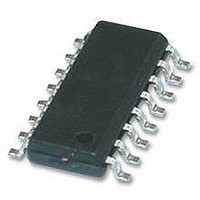
TEA1751LT/N1 NXP Semiconductors, TEA1751LT/N1 Datasheet - Page 5

TEA1751LT/N1
Manufacturer Part Number
TEA1751LT/N1
Description
AC-DC, PFC, FLYBACK, CNTRL, 16SOIC
Manufacturer
NXP Semiconductors
Datasheet
1.TEA1751LTN1518.pdf
(29 pages)
Specifications of TEA1751LT/N1
Input Voltage
276V
Output Current
1.2A
Output Voltage
11V
No. Of Outputs
2
Power Dissipation Pd
600mW
Voltage Regulator Case Style
SOIC
No. Of Pins
16
Operating Temperature Range
-40°C To
Supply Voltage Range
21V To 23V
Rohs Compliant
Yes
Lead Free Status / RoHS Status
Lead free / RoHS Compliant
Available stocks
Company
Part Number
Manufacturer
Quantity
Price
Company:
Part Number:
TEA1751LT/N1
Manufacturer:
SEIKO
Quantity:
55 000
Part Number:
TEA1751LT/N1
Manufacturer:
NXP/恩智浦
Quantity:
20 000
NXP Semiconductors
7. Functional description
TEA1751T_LT_2
Product data sheet
7.1.1 Start-up and UnderVoltage LockOut (UVLO)
7.1 General control
The TEA1751(L)T contains a controller for a power factor correction circuit as well as a
controller for a flyback circuit. A typical configuration is shown in
Initially the capacitor on the V
As long as V
is shorted to ground. For a short start-up time the charge current above V
until V
low again, ensuring a low duty cycle during fault conditions.
The control logic activates the internal circuitry and switches off the HV charge current
when the voltage on pin V
is activated and the soft start capacitors on the PFCSENSE and FBSENSE pins are
charged. When the LATCH pin voltage exceeds the V
capacitor on the PFCSENSE pin is charged, the PFC circuit is activated. Also the flyback
converter is activated (providing the soft start capacitor on the FBSENSE pin is charged).
The output voltage of the flyback converter is then regulated to its nominal output voltage.
The IC supply is taken over by the auxiliary winding of the flyback converter. See
If during start-up the LATCH pin does not reach the V
V
again.
Fig 3.
th(UVLO)
CC
, the LATCH pin output is deactivated and the charge current is switched on
reaches V
Typical configuration
CC
is below V
th(UVLO)
Rev. 02 — 23 December 2009
CC
trip
. If V
, the charge current is low. This protects the IC if the V
passes the V
CC
CC
pin is charged from the high voltage mains via the HV pin.
is between V
8
6
7
3
12
11
TEA1751(L)T
TEA1751T; TEA1751LT
startup
2
9
th(UVLO)
level. First, the LATCH pin current source
16 13
10
en(LATCH)
en(LATCH)
4
1
and V
GreenChip III SMPS control IC
startup
level before V
voltage and the soft start
Figure
, the charge current is
© NXP B.V. 2009. All rights reserved.
3.
trip
CC
is increased
014aaa301
reaches
Figure
CC
5 of 29
pin
4.


