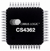
CS4362-KQZ Cirrus Logic Inc, CS4362-KQZ Datasheet - Page 29

CS4362-KQZ
Manufacturer Part Number
CS4362-KQZ
Description
IC,Audio Processor,QFP,48PIN,PLASTIC
Manufacturer
Cirrus Logic Inc
Datasheet
1.CS4362-KQZ.pdf
(42 pages)
Specifications of CS4362-KQZ
Number Of Bits
24
Data Interface
Serial
Number Of Converters
6
Voltage Supply Source
Analog and Digital
Power Dissipation (max)
390mW
Operating Temperature
-10°C ~ 70°C
Mounting Type
Surface Mount
Package / Case
48-LQFP
Lead Free Status / RoHS Status
Lead free / RoHS Compliant
Settling Time
-
Lead Free Status / RoHS Status
Lead free / RoHS Compliant, Lead free / RoHS Compliant
Other names
598-1644
Available stocks
Company
Part Number
Manufacturer
Quantity
Price
Company:
Part Number:
CS4362-KQZR
Manufacturer:
STM
Quantity:
2 332
DS257F2
6.6
6.7
6.8
variety of musical tastes and styles. The FILT_SEL bit is used to select which filter is used (see the control
port section for more details).
When in Stand-Alone Mode, only the “fast” roll-off filter is available.
Filter specifications can be found in
Clock Source Selection
The CS4362 has two serial clock and two left/right clock inputs. The SDINxCLK bits in the control port allow
the user to set which SCLK/LRCK pair is used to latch the data for each SDINx pin. The clocks applied to
LRCK1 and LRCK2 must be derived from the same MCLK and must be exact frequency multiples of each
other as specified in the
SCLK2/LRCK2, if either SCLK/LRCK pair loses synchronization then both SCLK/LRCK pairs will go through
a retime period where the device is re-evaluating clock ratios. During the retime period, all DAC pairs are
temporarily inactive, outputs are muted, and the mute control pins will go active according to the MUTEC
bits.
If unused, SCLK2 and LRCK2 should be tied static low and SDINx bits should all be set to SCLK1/LRCK1.
In Stand-Alone Mode, all DAC pairs use SCLK1 and LRCK1 for timing and SCLK2/LRCK2 should be tied
to ground.
Using DSD Mode
In Stand-Alone Mode, DSD operation is selected by holding DSD_EN(LRCK1) high and applying the DSD
data and clocks to the appropriate pins. The M2:0 pins set the expected DSD rate and MCLK ratio.
In Control-Port Mode, the FM bits set the device into DSD Mode (DSD_EN pin is not required to be held
high). The DIF register then controls the expected DSD rate and MCLK ratio. To access the full range of
DSD clocking modes (other than 64x DSD 4x MCLK and 128x DSD 2x MCLK), the following additional reg-
ister sequence needs to be written:
99h to register 00h
80h to register 1Ah
00h to register 00h
When exiting DSD Mode the following additional sequence needs to be written:
99h to register 00h
00h to register 1Ah
00h to register 00h
During DSD operation, the PCM related pins should either be tied low or remain active with clocks (except
LRCK1 in Stand-Alone Mode). When the DSD related pins are not being used, they should either be tied
static low or remain active with clocks (except M3 in Stand-Alone Mode).
Recommended Procedure for Switching Operational Modes
For systems where the absolute minimum in clicks and pops is required, it is recommended that the MUTE
bits are set prior to changing significant DAC functions (such as changing sample rates or clock sources).
The mute bits may then be released after clocks have settled and the proper CS4362 modes have been set.
It is required that the CS4362 be held in reset if the minimum high/low time specs of MCLK can not be met
during clock source changes.
“Switching Characteristics” on page
Section
1, and filter response plots can be found in
9. When using both SCLK1/LRCK1 and
Figures 9
CS4362
to 32.
29


