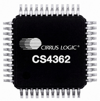
CS4362-KQZ Cirrus Logic Inc, CS4362-KQZ Datasheet - Page 30

CS4362-KQZ
Manufacturer Part Number
CS4362-KQZ
Description
IC,Audio Processor,QFP,48PIN,PLASTIC
Manufacturer
Cirrus Logic Inc
Datasheet
1.CS4362-KQZ.pdf
(42 pages)
Specifications of CS4362-KQZ
Number Of Bits
24
Data Interface
Serial
Number Of Converters
6
Voltage Supply Source
Analog and Digital
Power Dissipation (max)
390mW
Operating Temperature
-10°C ~ 70°C
Mounting Type
Surface Mount
Package / Case
48-LQFP
Lead Free Status / RoHS Status
Lead free / RoHS Compliant
Settling Time
-
Lead Free Status / RoHS Status
Lead free / RoHS Compliant, Lead free / RoHS Compliant
Other names
598-1644
Available stocks
Company
Part Number
Manufacturer
Quantity
Price
Company:
Part Number:
CS4362-KQZR
Manufacturer:
STM
Quantity:
2 332
30
7. CONTROL PORT INTERFACE
The control port is used to load all the internal settings. The operation of the control port may be completely asyn-
chronous with the audio sample rate. However, to avoid potential interference problems, the control port pins should
remain static if no operation is required.
The CS4362 has MAP auto increment capability, enabled by the INCR bit in the MAP register, which is the MSB. If
INCR is 0, then the MAP will stay constant for successive writes. If INCR is set to 1, then MAP will auto increment
after each byte is written from register 01h to 08h and then from 09h and 11h, allowing block reads or writes of suc-
cessive registers in two separate sections (the counter will not auto-increment to register 09h from register 08h).
7.1
7.2
7.3
7.3.1
7.3.2
Enabling the Control Port
On the CS4362 the control port pins are shared with stand-alone configuration pins. To enable the control
port, the user must set the CPEN bit. This is done by performing a I²C or SPI write. Once the control port is
enabled, these pins are dedicated to control port functionality.
To prevent audible artifacts the CPEN bit (see
Stand-Alone power-up sequence, approximately 1024 LRCK cycles. Writing this bit will halt the Stand-Alone
power-up sequence and initialize the control port to its default settings. Note, the CP_EN bit can be set any
time after RST goes high; however, setting this bit after the Stand-Alone power-up sequence has completed
can cause audible artifacts.
Format Selection
The control port has 2 formats: SPI and I²C, with the CS4362 operating as a slave device.
If I²C operation is desired, AD0/CS should be tied to VLC or GND. If the CS4362 ever detects a high to low
transition on AD0/CS after power-up and after the control port is activated, SPI format will be selected.
I²C Format
In I²C Format, SDA is a bidirectional data line. Data is clocked into and out of the part by the clock, SCL,
with a clock to data relationship as shown in Figure
edge (ACK) after each byte received. There is no CS pin. Pin AD0 forms the partial chip address and should
be tied to VLC or GND as required. The upper 6 bits of the 7 bit address field must be 001100.
Note:
Writing in I²C Format
To communicate with the CS4362, initiate a START condition of the bus. Next, send the chip address.
The eighth bit of the address byte is the R/W bit (low for a write). The next byte is the Memory Address
Pointer, MAP, which selects the register to be read or written. The MAP is then followed by the data to be
written. To write multiple registers, continue providing a clock and data, waiting for the CS4362 to ac-
knowledge between each byte. To end the transaction, send a STOP condition.
Reading in I²C Format
To communicate with the CS4362, initiate a START condition of the bus. Next, send the chip address.
The eighth bit of the address byte is the R/W bit (high for a read). The contents of the register pointed to
by the MAP will be output after the chip address. To read multiple registers, continue providing a clock
and issue an ACK after each byte. To end the transaction, send a STOP condition.
MCLK is required during all I²C transactions. Please see
tional information on the I²C Bus specification or visit http://www.semiconductors.philips.com.
Section
Figure
4.1.1) should be set prior to the completion of the
7. The receiving device should send an acknowl-
“References” on page 40
to obtain addi-
CS4362
DS257F2


