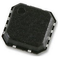
AD8337BCPZ Analog Devices Inc, AD8337BCPZ Datasheet

AD8337BCPZ
Specifications of AD8337BCPZ
Available stocks
Related parts for AD8337BCPZ
AD8337BCPZ Summary of contents
Page 1
FEATURES Low noise Voltage noise = 2.2 nV/√Hz Current noise = 4.8 pA/√Hz (positive input) Wide bandwidth (−3 dB) = 280 MHz Nominal gain range (preamp gain = 6 dB) Gain scaling: 19.7 dB/V DC-coupled ...
Page 2
AD8337 TABLE OF CONTENTS Features .............................................................................................. 1 Applications....................................................................................... 1 Functional Block Diagram .............................................................. 1 General Description ......................................................................... 1 Revision History ............................................................................... 2 Specifications..................................................................................... 3 Absolute Maximum Ratings............................................................ 5 ESD Caution.................................................................................. 5 Pin Configuration and Function Descriptions............................. 6 Typical Performance Characteristics ...
Page 3
SPECIFICATIONS V = ±2 25°C, PrA Gain = + otherwise specified. Table 1. Parameter GENERAL PARAMETERS –3 dB Small Signal Bandwidth –3 dB Large Signal Bandwidth Slew Rate Input Voltage Noise Input Current Noise ...
Page 4
AD8337 Parameter DYNAMIC PERFORMANCE Harmonic Distortion HD2 HD3 HD2 HD3 HD2 HD3 Input 1 dB Compression Point Two-Tone Intermodulation Distortion (IMD3) Output Third-Order Intercept Overload Recovery ACCURACY Absolute Gain Error GAIN CONTROL INTERFACE Gain Scaling Factor Gain Range Intercept Input ...
Page 5
ABSOLUTE MAXIMUM RATINGS Table 2. Parameter Voltage Supply Voltage (VPOS, VNEG) Input Voltage (INPx) GAIN Voltage Power Dissipation (Exposed Pad Soldered to PC Board) Temperature Operating Temperature Range Storage Temperature Range Lead Temperature (Soldering, 60 sec) Thermal Data—4-Layer JEDEC Board ...
Page 6
AD8337 PIN CONFIGURATION AND FUNCTION DESCRIPTIONS Table 3. Pin Function Descriptions Pin No. Mnemonic Description 1 VOUT VGA Output. 2 VCOM Common Ground when using Plus and Minus Supply Voltages. For single-supply operation, provide half the positive supply voltage at ...
Page 7
TYPICAL PERFORMANCE CHARACTERISTICS = ±2 25° 500 Ω, including a 20 Ω snubbing resistor MHz configuration, unless otherwise noted. 30 +85°C +25°C 25 –40° ...
Page 8
AD8337 +0.7 GAIN V = +0.5 GAIN +0.2 GAIN GAIN –0.2 GAIN –0.5 GAIN –0.7 GAIN –5 100k 1M 10M ...
Page 9
– ±2.5V S –4 –6 +85°C –8 +25°C –40°C –10 –800 –600 –400 –200 0 200 V (mV) GAIN Figure 15. Offset Voltage vs Three Temperatures GAIN See Figure ...
Page 10
AD8337 10MHz 0.7V GAIN INPUT REFERRED NOISE 1 R THERMAL NOISE ALONE S 0 SOURCE RESISTANCE (Ω) Figure 21. Input-Referred Noise vs. R See Figure 61 35 50Ω SOURCE 30 25 WITH 50Ω ...
Page 11
p-p OUT p-p OUT V = 0.5V p-p OUT –40 LIMITED BY MAXIMUM PREAMP OUTPUT SWING –50 –60 –70 –80 –90 –800 –600 –400 –200 0 200 400 V (mV) GAIN Figure 27. ...
Page 12
AD8337 0.7V GAIN –20 INPUT –40 OUTPUT –60 –80 –20 – TIME (ns) Figure 33. Small Signal Pulse Response See Figure 0.7V GAIN 60 INPUT ...
Page 13
V = 0.7V GAIN 1.0 0.5 0 –0.5 –1.0 –1.5 –0.3 –0.1 0.1 0.3 0.5 0.7 0.9 1.1 TIME (µs) Figure 39. Preamp Overdrive Recovery See Figure 55 1 0.7V GAIN 1.0 0.5 0 –0.5 –1.0 –1.5 ...
Page 14
AD8337 TEST CIRCUITS NETWORK ANALYZER OUT IN 50Ω 50Ω AD8337 + 3 PRA 49.9Ω – 100Ω V GAIN 100Ω Figure 44. Gain and Gain Error vs. V NETWORK ANALYZER OUT IN 50Ω 50Ω AD8337 + 3 49.9Ω ...
Page 15
SPECTRUM ANALYZER IN 50Ω AD8337 + 3 PRA 1 49.9Ω – 100Ω V GAIN 100Ω Figure 50. Input-Referred and Output-Referred Noise NOISE FIGURE METER NOISE SOURCE INPUT DRIVE NOISE SOURCE AD8337 3 + 49.9Ω PRA 1 (OR ...
Page 16
AD8337 FUNCTION GENERATOR OSCILLOSCOPE POWER SPLITTER OUTPUT CH1 50Ω AD8337 + 3 PRA 49.9Ω – 100Ω 100Ω Figure 56. VGA Overdrive Recovery DMM (+I) 8 AD8337 + 3 PRA – 100Ω DMM 100Ω (–I) ...
Page 17
SPECTRUM ANALYZER IN 50Ω AD8337 3 + PRA 1 4 – 100Ω 0.7V 100Ω Figure 62. Short-Circuit Input Noise vs. Frequency +22dB –6dB SIGNAL GENERATOR +22dB –6dB SIGNAL GENERATOR NETWORK ANALYZER 22dB OUT + 3 PRA 49.9Ω – ...
Page 18
AD8337 THEORY OF OPERATION R G OVERVIEW The AD8337 is a low noise, single-ended, linear-in-dB, general- purpose, variable gain amplifier (VGA) usable at frequencies up to 100 MHz fabricated using a proprietary Analog Devices dielectrically isolated, complementary bipolar ...
Page 19
The gain scaling factor (gain slope) is designed for 20 dB/V; this relatively low slope ensures that noise on the GAIN input is not unduly amplified. Because a VGA functions as a multiplier important to make sure that ...
Page 20
AD8337 APPLICATIONS PREAMPLIFIER CONNECTIONS Noninverting Gain Configuration The AD8337 preamplifier is an uncommitted, current-feedback op amp that is stable for values of R ≥ 100 Ω. See Figure 66 FB2 for the noninverting feedback connections. PREAMPLIFIER INPP + 3 R ...
Page 21
In the time domain, stray capacitance at the output pin can induce overshoot on the edges of transient signals, as seen in Figure 70 and Figure 72. The amplitude of the overshoot is also a function of the slewing of ...
Page 22
AD8337 The offset voltage effect of the AD8337, as with all VGAs, can appear as a complex waveform when observed across the range of V voltage. Generated by multiple sources, each device has GAIN a unique V profile while the ...
Page 23
RVO1 VOUT 453Ω TP1 RVO3 0Ω 0Ω R2 49.9Ω R5 Figure 76. Evaluation Board Schematic—Noninverting Configuration Figure 77. Evaluation Board—Component Side Copper GND1 GND2 GND3 GND4 + 10µF L2 120nH 0.1µF ...
Page 24
... AD8337BCPZ-R2 −40°C to +85°C 1 AD8337BCPZ-REEL −40°C to +85°C 1 AD8337BCPZ-REEL7 −40°C to +85°C 1 AD8337BCPZ-WP −40°C to +85°C 1 AD8337-EVALZ AD8337-EVAL-INV AD8337-EVAL- Pb-free part. ©2005-2007 Analog Devices, Inc. All rights reserved. Trademarks and registered trademarks are the property of their respective owners. ...


