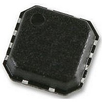
AD8337BCPZ Analog Devices Inc, AD8337BCPZ Datasheet - Page 20

AD8337BCPZ
Manufacturer Part Number
AD8337BCPZ
Description
VGA, DC COUPLED, SMD, LFCSP-8, 8337
Manufacturer
Analog Devices Inc
Datasheet
1.AD8337BCPZ.pdf
(24 pages)
Specifications of AD8337BCPZ
No. Of Amplifiers
1
Bandwidth
280MHz
Gain Accuracy
3.5dB
No. Of Channels
1
Supply Voltage Range
4.5V To 10V
Amplifier Case Style
LFCSP
No. Of Pins
8
Operating Temperature Range
-40°C To
Lead Free Status / RoHS Status
Lead free / RoHS Compliant
Available stocks
Company
Part Number
Manufacturer
Quantity
Price
Company:
Part Number:
AD8337BCPZ
Manufacturer:
ADI
Quantity:
104
Company:
Part Number:
AD8337BCPZ-WP
Manufacturer:
STM
Quantity:
2 483
AD8337
APPLICATIONS
PREAMPLIFIER CONNECTIONS
Noninverting Gain Configuration
The AD8337 preamplifier is an uncommitted, current-feedback
op amp that is stable for values of R
for the noninverting feedback connections.
Two surface-mount resistors establish the preamplifier gain.
Equal values of 100 Ω configure the preamplifier for a 6 dB gain
and the device for a default gain range of 0 dB to 24 dB.
For preamp gains ≥2, select a value of R
R
increase the offset voltage, but smaller values compromise
stability. If R
referred noise decreases.
Inverting Gain Configuration
For applications requiring polarity inversion of negative pulses, or
for waveforms that require current sinking, the preamplifier can
be configured as an inverting gain amplifier. When configured
with bipolar supplies, the preamplifier amplifies positive or
negative input voltages with no level shifting of the common-
mode input voltage required. Figure 67 shows the AD8337
configured for inverting gain operation.
Because the AD8337 is a very high frequency device, stability
issues can occur unless the circuit board on which it is used is
carefully laid out. The stability of the preamp is affected by
parasitic capacitance around the INPN pin. Position the pre-
amp gain resistors, R
INPN, to minimize stray capacitance.
FB1
≤ 100 Ω. Higher values of R
Figure 66. AD8337 Preamplifier Configured for Noninverting Gain
Figure 67. The AD8337 Preamplifier Configured for Inverting Gain
R
FB1
G
≤ 100 Ω, the gain increases and the input-
R
FB1
FB1
R
R
FB1
R
PRAO
FB2
and R
PRAO
INPP
INPP
INPN
FB2
INPN
3
4
5
3
4
5
FB2
, as close as possible to Pin 4,
FB2
PREAMPLIFIER
PREAMPLIFIER
+
–
+
–
reduce the bandwidth and
FB2
≥ 100 Ω. See Figure 66
FB2
≥ 100 Ω and
Rev. B | Page 20 of 24
DRIVING CAPACITIVE LOADS
Because of the large bandwidth of the AD8337, stray
capacitance at the output pin can induce peaking in the
frequency response as the gain of the amplifier begins to roll off.
Figure 68 shows peaking with two values of load capacitance
using ±2.5 V supplies and V
Figure 68. Peaking in the Frequency Response for Two Values of Output
Figure 69. Frequency Response for Two Values of Output Capacitance
Capacitance with ±2.5 V Supplies and No Snubbing Resistor
25
20
15
10
–5
25
20
15
10
–5
100k
5
0
100k
5
0
NO SNUBBING RESISTOR
V
V
WITH 20Ω SNUBBING RESISTOR
GAIN
GAIN
C
C
C
C
C
C
L
L
L
L
L
L
= 0pF
= 10pF
= 22pF
= 0pF
= 10pF
= 22pF
= 0V
= 0V
with a 20 Ω Snubbing Resistor
1M
1M
FREQUENCY (Hz)
FREQUENCY (Hz)
GAIN
= 0 V.
10M
10M
100M
100M
500M
500M


