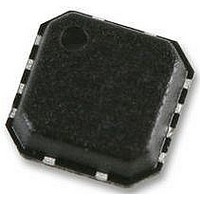
AD8337BCPZ Analog Devices Inc, AD8337BCPZ Datasheet - Page 18

AD8337BCPZ
Manufacturer Part Number
AD8337BCPZ
Description
VGA, DC COUPLED, SMD, LFCSP-8, 8337
Manufacturer
Analog Devices Inc
Datasheet
1.AD8337BCPZ.pdf
(24 pages)
Specifications of AD8337BCPZ
No. Of Amplifiers
1
Bandwidth
280MHz
Gain Accuracy
3.5dB
No. Of Channels
1
Supply Voltage Range
4.5V To 10V
Amplifier Case Style
LFCSP
No. Of Pins
8
Operating Temperature Range
-40°C To
Lead Free Status / RoHS Status
Lead free / RoHS Compliant
Available stocks
Company
Part Number
Manufacturer
Quantity
Price
Company:
Part Number:
AD8337BCPZ
Manufacturer:
ADI
Quantity:
104
Company:
Part Number:
AD8337BCPZ-WP
Manufacturer:
STM
Quantity:
2 483
AD8337
THEORY OF OPERATION
OVERVIEW
The AD8337 is a low noise, single-ended, linear-in-dB, general-
purpose, variable gain amplifier (VGA) usable at frequencies
up to 100 MHz. It is fabricated using a proprietary Analog
Devices dielectrically isolated, complementary bipolar process.
The bandwidth is dc to 280 MHz and features low dc offset
voltage and an ideal nominal gain range of 0 dB to 24 dB.
Requiring about 15.5 mA, the power consumption is only
78 mW from either a single +5 V or a dual ±2.5 V supply.
Figure 65 is the circuit block diagram of the AD8337.
PREAMPLIFIER
An uncommitted, current-feedback op amp included in the
AD8337 can be used as a preamplifier to buffer the ladder
network attenuator of the X-AMP. As with any op amp, the gain
is established using external resistors, and the preamplifier is
specified with a noninverting gain of 6 dB (2×) and gain resistor
values of 100 Ω. The preamplifier gain can be increased using
larger values of R
The value of R
compensation capacitor determines the 3 dB bandwidth, and
smaller values can compromise preamplifier stability.
Because the AD8337 is dc-coupled, larger preamp gains increase
the offset voltage. The offset voltage can be compensated by
connecting a resistor between the INPN input and the supply
voltage. If the offset is negative, the resistor value connects to the
negative supply. For ease of adjustment, a trimmer network
can be used.
For larger gains, the overall noise is reduced if a low value of
R
preamp gain is 16× (24.1 dB), and the input-referred noise is
approximately 1.5 nV/√Hz. For this value of gain, the overall
gain range increases by 18 dB; therefore, the gain range is
18 dB to 42 dB.
FB1
is selected. For values of R
FB2
FB2
should be ≥100 Ω because it and an internal
, trading off bandwidth and offset voltage.
FB1
R
= 20 Ω and R
G
R
R
FB1
INPP
INPN
PRAO
FB2
FB2
3
4
5
= 301 Ω, the
R
FB1
+
–
PRA
6dB
= R
BIAS
FB2
VCOM
Figure 65. Block Diagram
= 100Ω
Rev. B | Page 18 of 24
2
INTERPOLATOR
–24dB TO 0dB
+
ATTENUATOR
–
VPOS
VNEG
8
6
VGA
This X-AMP, with its linear-in-dB gain characteristic
architecture, yields the optimum dynamic range for receiver
applications. Referring to Figure 65, the signal path consists
of a −24 dB variable attenuator followed by a fixed gain amplifier
of 18 dB, for a total VGA gain range of −6 dB to +18 dB. With
the preamplifier configured for a gain of 6 dB, the composite
gain range is 0 dB to 24 dB.
The VGA plus preamp with 6 dB of gain implements the
following exact gain law
where the nominal intercept (ICPT) is 12.65 dB.
The ICPT increases as the gain of the preamp is increased. For
example, if the gain of the preamp is increased by 6 dB, ICPT
increases to 18.65 dB. Although the previous equation shows
the exact gain law as based on statistical data, a quick estimation
of signal levels can be made using the default slope of 20 dB/V
for a particular gain setting. For example, the change in gain for
a V
5.91 dB using the exact slope of 19.6 dB/V. This is a difference
of only 0.09 dB.
GAIN CONTROL
The gain control interface provides a high impedance input
and is referenced to VCOM pin (in a single-supply application
to midsupply at [VPOS + VNEG]/2 for optimum swing).
When dual supplies are used, VCOM is connected to ground.
The voltage on the VCOM pin determines the midpoint of the
gain range. For a ground referenced design, the V
from −0.7 V to +0.7 V with the most linear-in-dB section of the
gain control between −0.6 V and +0.6 V. In the center 80% of
the V
gain control voltage can be increased or decreased to the positive
or negative rails without gain foldover.
GAIN
Gain
GAIN
change of 0.3 V is 6 dB using a slope of 20 dB/V and
INTERFACE
range, the gain error is typically less than ±0.2 dB. The
(dB)
+
–
18dB
(8X)
GAIN
GAIN
7
=
749Ω
107Ω
⎡
⎢ ⎣
19.7
dB
V
1
VOUT
×
V
GAIN
⎤
⎥ ⎦
+
ICPT
(dB)
GAIN
range is


