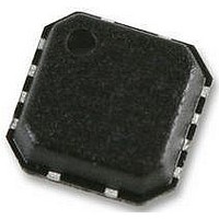
AD8337BCPZ Analog Devices Inc, AD8337BCPZ Datasheet - Page 21

AD8337BCPZ
Manufacturer Part Number
AD8337BCPZ
Description
VGA, DC COUPLED, SMD, LFCSP-8, 8337
Manufacturer
Analog Devices Inc
Datasheet
1.AD8337BCPZ.pdf
(24 pages)
Specifications of AD8337BCPZ
No. Of Amplifiers
1
Bandwidth
280MHz
Gain Accuracy
3.5dB
No. Of Channels
1
Supply Voltage Range
4.5V To 10V
Amplifier Case Style
LFCSP
No. Of Pins
8
Operating Temperature Range
-40°C To
Lead Free Status / RoHS Status
Lead free / RoHS Compliant
Available stocks
Company
Part Number
Manufacturer
Quantity
Price
Company:
Part Number:
AD8337BCPZ
Manufacturer:
ADI
Quantity:
104
Company:
Part Number:
AD8337BCPZ-WP
Manufacturer:
STM
Quantity:
2 483
In the time domain, stray capacitance at the output pin can
induce overshoot on the edges of transient signals, as seen in
Figure 70 and Figure 72. The amplitude of the overshoot is
also a function of the slewing of the transient (not shown).
The transition time of the input pulses used for Figure 70
and Figure 72 was set deliberately high at 300 ps to demonstrate
the fast response time of the amplifier. Signals with longer
transition times generate less overshoot.
–200
–400
–600
–800
–200
–400
–600
–800
–200
–400
–600
–800
Figure 70. Pulse Response for Two Values of Output Capacitance
Figure 71. Pulse Response for Two Values of Output Capacitance
Figure 72. Large Signal Pulse Response for Two Values of Output
800
600
400
200
800
600
400
200
800
600
400
200
0
0
–20
0
–20
Capacitance with ±5 V Supplies and No Snubbing Resistor
–20
INPUT
INPUT
OUTPUT
V
OUTPUT
with ±2.5 V Supplies and a 20 Ω Snubbing Resistor
OUTPUT
S
INPUT
–10
–10
with ±2.5 V Supplies and No Snubbing Resistor
–10
= ±5V
0
0
0
WITH NO SNUBBING RESISTOR
WITH 20Ω SNUBBING RESISTOR
C
C
C
NO SNUBBING RESISTOR
C
C
C
10
10
L
L
L
10
L
L
L
= 10pF
C
C
C
= 0pF
= 22pF
= 0pF
= 10pF
= 22pF
L
L
L
= 0pF
= 10pF
= 22pF
20
20
20
TIME (ns)
TIME (ns)
TIME (ns)
30
30
30
40
40
40
50
50
50
60
60
60
70
70
70
80
80
80
–40
80
60
40
20
0
–20
–60
–80
80
60
40
20
0
–20
–40
–60
–80
80
60
40
20
0
–20
–40
–60
–80
Rev. B | Page 21 of 24
The effects of stray output capacitance are mitigated with a
small value snubbing resistor, R
as near as possible to, the output pin.
Figure 73
a 20 Ω snubbing resistor. R
ratio of R
high impedance loads, such as ADCs. For other loads, alternate
values of R
curves in the Typical Performance Characteristics section of this
data sheet are derived using a 20 Ω snubbing resistor.
The best way to avoid the effects of stray capacitance is to
exercise care in PC board layout. Locate the passive components
or devices connected to the AD8337 output pins as close as
possible to the package.
Although a nonissue, the preamplifier output is also sensitive
to load capacitance. However, the series connection of R
and R
If overshoot appears, it can be mitigated in the same way as the
VGA output, by inserting a snubbing resistor.
GAIN CONTROL CONSIDERATIONS
In typical applications, voltages applied to the GAIN input are dc
or relatively low frequency signals. The high input impedance of
the AD8337 enables several devices to be connected in parallel.
This is useful for arrays of VGAs, such as those used for calibra-
tion adjustments.
Under dc or slowly changing ramp conditions, the gain tracks
the gain control voltage as shown in Figure 3. However, it is
often necessary to consider other effects influenced by the
V
GAIN
–200
–400
–600
–800
Figure 73. Pulse Response for Two Values of Output Capacitance
800
600
400
200
FB2
input.
0
–20
is typically the only load connected to the preamplifier.
LOAD
V
INPUT
OUTPUT
show the improvement in dynamic performance with
S
SNUB
= ±5V
with ±5 V Supplies and a 20 Ω Snubbing Resistor
–10
/(R
can be determined empirically. The data for the
SNUB
0
WITH 20Ω SNUBBING RESISTOR
+ R
C
C
C
10
L
L
L
= 0pF
= 10pF
= 22pF
LOAD
20
SNUB
), a very small loss when used with
TIME (ns)
B
reduces the gain slightly by the
30
SNUB
, placed in series with, and
B
40
Figure 69 Figure 71
50
60
,
70
AD8337
80
80
60
40
20
0
–20
–40
–60
–80
FB1
, and


