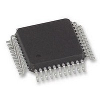
FM6124-QG Ramtron, FM6124-QG Datasheet - Page 35

FM6124-QG
Manufacturer Part Number
FM6124-QG
Description
FRAM, 24KB, EVENT DATA REC, QFP44
Manufacturer
Ramtron
Datasheet
1.FM6124-QG.pdf
(53 pages)
Specifications of FM6124-QG
Memory Size
24KB
Nvram Features
RTC
Supply Voltage Range
3V To 3.6V
Memory Case Style
QFP
No. Of Pins
44
Operating Temperature Range
-40°C To +85°C
Package / Case
QFP
Interface
I2C
Memory
RoHS Compliant
Interface Type
I2C, Serial, 2-Wire
Rohs Compliant
Yes
Access Time
100 KBPs
Operating Supply Voltage
3 V to 3.6 V
Mounting Style
SMD/SMT
Lead Free Status / Rohs Status
Details
Available stocks
Company
Part Number
Manufacturer
Quantity
Price
Company:
Part Number:
FM6124-QG
Manufacturer:
ABOV
Quantity:
3 000
Electrical Specifications
Absolute Maximum Ratings
Stresses above those listed under Absolute Maximum Ratings may cause permanent damage to the device. This is a stress rating
only, and the functional operation of the device at these or any other conditions above those listed in the operational section of this
specification is not implied. Exposure to absolute maximum ratings conditions for extended periods may affect device reliability.
DC Operating Conditions (
Rev. 4.0 (EOL)
July 2010
Symbol
V
I
I
V
I
I
V
V
V
V
V
V
I
I
V
V
DD
SB
BAK
BAKTC
LI
LO
DD
BAK
TP0
TP1
TP2
TP3
RST
SW
IL
IH
Symbol
T
V
V
T
V
V
LEAD
BAK
STG
ESD
DD
IN
Main Power Supply
Standby Current
RTC Backup Voltage
RTC Backup Current
Trickle Charge Current with V
V
RTC, VTP(1:0) = 00b
V
RTC, VTP(1:0) = 01b
V
RTC, VTP(1:0) = 10b
V
RTC, VTP(1:0) = 11b
Battery Switchover Voltage
Input Leakage Current
Output Leakage Current
Input Low Voltage
Input High Voltage
Trickle Charger Off
Fast Charge Off (FC = 0)
Fast Charge On (FC = 1)
V
DD
DD
DD
DD
V
V
All inputs except as listed below
CNT battery-backed (V
All inputs except as listed below
CNT battery-backed (V
CNT (V
CNT V
PFI
DD
BAK
BAK
Trip Point Voltage for MCU companion &
Trip Point Voltage for MCU companion &
Trip Point Voltage for MCU companion &
Trip Point Voltage for MCU companion &
Supply Current (VBC=0)
> V
< V
Power Supply Voltage with respect to V
Voltage on any signal pin with respect to V
Backup Supply Voltage
Storage Temperature
Lead Temperature (Soldering, 10 seconds)
Electrostatic Discharge Voltage
Package Moisture Sensitivity Level
DD
- Human Body Model
- Charged Device Model
- Machine Model
DD
BAK
BAK
> V
> V
min
min
SW
T
SW
A
Parameter
)
= -40° C to + 85° C, V
(VBC=0)
DD
DD
< V
< V
(JEDEC Std JESD22-A115-A)
Description
BAK
SW
SW
(JEDEC Std JESD22-A114-E)
=0V
)
)
(JEDEC Std JESD22-C101-C)
DD
= 3.0V to 3.6V unless otherwise specified)
SS
V
0.7 V
0.7 V
BAK
SS
Min
2.55
2.70
2.80
2.93
200
-0.3
-0.3
-0.3
3.0
2.0
1.6
2.0
50
0
-
– 0.5
DD
DD
2.75
Typ
3.0
2.6
2.9
3.0
-
-1.0V to +5.0V and
-55°C to + 125°C
V
-1.0V to +3.6V
-1.0V to +4.5V
IN
V
V
V
V
Continued
Ratings
< V
0.3 V
300° C
MSL-3
BAK
DD
DD
DD
TBD
TBD
TBD
2500
TBD
TBD
Max
2.70
2.85
2.97
3.13
200
3.6
3.6
2.7
0.5
0.8
50
1
DD
+ 0.3
+ 0.3
+ 0.3
+ 0.3
DD
+1.0V
>>
Units
mA
µA
µA
µA
µA
µA
µA
V
V
V
V
V
V
V
V
V
V
V
V
V
V
V
V
Page 35 of 53
Notes
1
3
4
5
6
7
7
7
7


