FM6124-QG Ramtron, FM6124-QG Datasheet - Page 36
FM6124-QG
Manufacturer Part Number
FM6124-QG
Description
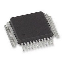
FRAM, 24KB, EVENT DATA REC, QFP44
Manufacturer
Ramtron
Datasheet
1.FM6124-QG.pdf
(53 pages)
Specifications of FM6124-QG
Memory Size
24KB
Nvram Features
RTC
Supply Voltage Range
3V To 3.6V
Memory Case Style
QFP
No. Of Pins
44
Operating Temperature Range
-40°C To +85°C
Package / Case
QFP
Interface
I2C
Memory
RoHS Compliant
Interface Type
I2C, Serial, 2-Wire
Rohs Compliant
Yes
Access Time
100 KBPs
Operating Supply Voltage
3 V to 3.6 V
Mounting Style
SMD/SMT
Lead Free Status / Rohs Status
Details
Available stocks
Company
Part Number
Manufacturer
Quantity
Price
Company:

Part Number:
FM6124-QG
Manufacturer:
ABOV
Quantity:
3 000


Notes
1.
2.
3.
4.
5.
6.
7.
AC Parameters
All SCL specifications as well as start and stop conditions apply to both read and write operations.
Supervisor Timing (T
Notes
1
2
3
4
Rev. 4.0 (EOL)
July 2010
DC Operating Conditions, continued
Symbol
V
V
R
V
V
Symbol
f
t
t
t
t
t
t
t
t
t
t
t
t
t
t
t
t
t
t
f
Symbol
LOW
HIGH
AA
BUF
HD:STA
SU:STA
HD:DAT
SU:DAT
R
F
SU:STO
DH
RPW
RNR
VR
VF
WDST
WDET
SCL
CNT
RSTB
OL
OH
PFI
HYS
Full complete operation. Supervisory circuits, RTC, etc operate to lower voltages as specified.
All inputs at V
The VBAK trickle charger automatically regulates the maximum voltage on this pin for capacitor backup applications.
V
V
This is the V
The minimum V
This parameter is characterized but not tested.
Slope measured at any point on V
t
satisfied. The StartTime has a resolution of 25ms. The EndTime has a resolution of 60ms.
The RSTB pin will drive low for this amount of time after the internal reset circuit is activated due to a watchdog, low
voltage, or manual reset event.
DOG1
BAK
BAK
is the programmed StartTime and t
= 3.0V, V
will source current when trickle charge is enabled (VBC bit=1), V
Parameter
Output Low Voltage @ I
Output High Voltage
Pull-up resistance for RSTB inactive
Power Fail Input Reference Voltage
Power Fail Input (PFI) Hysteresis (Rising)
Parameter
SCL Clock Frequency
Clock Low Period
Clock High Period
SCL Low to SDA Data Out Valid
Bus Free Before New Transmission
Start Condition Hold Time
Start Condition Setup for Repeated Start
Data In Hold Time
Data In Setup Time
Input Rise Time
Input Fall Time
Stop Condition Setup Time
Data Output Hold
(PFO) @ I
Parameter
RSTB Pulse Width (active low time)
RSTB Response Time to V
V
V
Watchdog StartTime
Watchdog EndTime
Frequency of Event Counter
DD
DD
DD
(T
SS
Rise Time
Fall Time
supply current contributed by enabling the trickle charger circuit, and does not account for I
DD
A
DD
or V
= -40° C to + 85° C, V
< V
to guarantee the level of RSTB remains a valid V
A
OH
DD,
= -40° C to + 85° C, V
SW
= -2 mA
static. Trickle charger off (VBC=0).
, oscillator running, CNT at VBAK.
(from SCL @ VIL)
DD
OL
waveform.
= 3 mA
(T
DD
DOG2
DD
A
<V
= 3.0V to 3.6V, C
= -40° C to + 85° C, V
is the programmed EndTime in registers 0Bh and 0Ch, V
TP
DD
(noise filter)
= 3.0V to 3.6V)
L
= 100 pF unless otherwise specified)
V
TBD
Min
4.7
4.0
4.7
4.0
4.7
4.0
DD
1.475
DD
0
0
0
Min
50
OL
-
– 0.8
= 3.0V to 3.6V unless otherwise specified)
level.
DD
0.3*t
t
Min
> V
100
DOG2
30
50
Max
TBD
TBD
7
0
100
DOG1
3
BAK
1.50
Typ
, and V
-
Units
3.3*t
kHz
µs
µs
µs
µs
µs
µs
ns
ns
ns
ns
µs
ns
Max
t
TBD
BAK
100
DOG1
25
-
-
DOG2
1.525
< V
Max
400
100
0.4
-
Notes
BAK
1
1
max.
Units
µs/V
µs/V
DD
kHz
ms
ms
ms
µs
> V
Units
BAKTC
mV
KΩ
V
V
V
TP
, and t
.
Notes
Page 36 of 53
1,2
1,2
Notes
1
3
3
RPU
Related parts for FM6124-QG
Image
Part Number
Description
Manufacturer
Datasheet
Request
R

Part Number:
Description:
Event Data Recorder With F-ram
Manufacturer:
Ramtron Corporation
Datasheet:

Part Number:
Description:
SOP28
Manufacturer:
Ramtron
Datasheet:
Part Number:
Description:
SOP-28
Manufacturer:
Ramtron
Datasheet:
Part Number:
Description:
SOP-28
Manufacturer:
Ramtron
Datasheet:
Part Number:
Description:
SOP-28
Manufacturer:
Ramtron
Datasheet:
Part Number:
Description:
TSOP44
Manufacturer:
Ramtron
Datasheet:
Part Number:
Description:
SOP8
Manufacturer:
Ramtron
Datasheet:
Part Number:
Description:
SOP8
Manufacturer:
Ramtron
Datasheet: