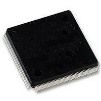
LFXP2-17E-5QN208C8W LATTICE SEMICONDUCTOR, LFXP2-17E-5QN208C8W Datasheet - Page 20

LFXP2-17E-5QN208C8W
Manufacturer Part Number
LFXP2-17E-5QN208C8W
Description
FPGA, 17K LUTS, 146 IO, DSP, 208PQFP
Manufacturer
LATTICE SEMICONDUCTOR
Series
LatticeXP2r
Datasheet
1.LFXP2-5E-5TN144C.pdf
(93 pages)
Specifications of LFXP2-17E-5QN208C8W
No. Of Macrocells
8500
Family Type
LatticeXP2
No. Of Speed Grades
5
No. Of I/o's
146
Clock Management
PLL
Core Supply Voltage Range
1.14V To 1.26V
I/o Supply
RoHS Compliant
- Current page: 20 of 93
- Download datasheet (2Mb)
Lattice Semiconductor
EBR memory supports three forms of write behavior for single port or dual port operation:
1. Normal – Data on the output appears only during a read cycle. During a write cycle, the data (at the current
2. Write Through – A copy of the input data appears at the output of the same port during a write cycle. This mode
3. Read-Before-Write – When new data is being written, the old content of the address appears at the output.
Memory Core Reset
The memory array in the EBR utilizes latches at the A and B output ports. These latches can be reset asynchro-
nously or synchronously. RSTA and RSTB are local signals, which reset the output latches associated with Port A
and Port B respectively. GSRN, the global reset signal, resets both ports. The output data latches and associated
resets for both ports are as shown in Figure 2-17.
Figure 2-17. Memory Core Reset
For further information on the sysMEM EBR block, please see TN1137, LatticeXP2 Memory Usage Guide.
EBR Asynchronous Reset
EBR asynchronous reset or GSR (if used) can only be applied if all clock enables are low for a clock cycle before the
reset is applied and released a clock cycle after the low-to-high transition of the reset signal, as shown in Figure 2-18.
The GSR input to the EBR is always asynchronous.
Figure 2-18. EBR Asynchronous Reset (Including GSR) Timing Diagram
address) does not appear on the output. This mode is supported for all data widths.
is supported for all data widths.
This mode is supported for x9, x18 and x36 data widths.
GSRN
RSTA
RSTB
Programmable Disable
Reset
Clock
Clock
Enable
Memory Core
2-17
Output Data
L
L
D
D
Latches
CLR
CLR
SET
SET
Q
Q
LatticeXP2 Family Data Sheet
Port A[17:0]
Port B[17:0]
Architecture
Related parts for LFXP2-17E-5QN208C8W
Image
Part Number
Description
Manufacturer
Datasheet
Request
R

Part Number:
Description:
IC, LATTICEXP2 FPGA, 435MHZ, FPBGA-484
Manufacturer:
LATTICE SEMICONDUCTOR
Datasheet:

Part Number:
Description:
Development Tools & Eval/Demo Boards
Manufacturer:
LATTICE SEMICONDUCTOR
Datasheet:
Part Number:
Description:
FPGA LatticeXP2 Family 17000 Cells Flash Technology 1.2V 484-Pin FBGA
Manufacturer:
LATTICE SEMICONDUCTOR
Datasheet:
Part Number:
Description:
FPGA LatticeXP2 Family 17000 Cells Flash Technology 1.2V 484-Pin FBGA
Manufacturer:
LATTICE SEMICONDUCTOR
Datasheet:
Part Number:
Description:
FPGA LatticeXP2 Family 17000 Cells Flash Technology 1.2V 484-Pin FBGA
Manufacturer:
LATTICE SEMICONDUCTOR
Datasheet:
Part Number:
Description:
Latticexp2 Fpga Data Sheets
Manufacturer:
Lattice Semiconductor Corp.
Datasheet:

Part Number:
Description:
FPGA - Field Programmable Gate Array 5K LUTs 146I/O Inst- on DSP 1.2V -5 Spd
Manufacturer:
Lattice
Datasheet:

Part Number:
Description:
FPGA - Field Programmable Gate Array 5K LUTs 172I/O Inst- on DSP 1.2V -5 Spd
Manufacturer:
Lattice
Datasheet:

Part Number:
Description:
FPGA - Field Programmable Gate Array 5K LUTs 100I/O Inst- on DSP 1.2V -5 Spd
Manufacturer:
Lattice
Datasheet:
Part Number:
Description:
ISPLSI2032-80LT44Lattice Semiconductor [In-System Programmable High Density PLD]
Manufacturer:
Lattice Semiconductor Corp.
Datasheet:
Part Number:
Description:
IC PROGRAMMED LATTICE GAL 16V8
Manufacturer:
Lattice Semiconductor Corp.
Datasheet:
Part Number:
Description:
357-036-542-201 CARDEDGE 36POS DL .156 BLK LOPRO
Manufacturer:
Lattice Semiconductor Corp.
Datasheet:
Part Number:
Description:
357-036-542-201 CARDEDGE 36POS DL .156 BLK LOPRO
Manufacturer:
Lattice Semiconductor Corp.
Datasheet:
Part Number:
Description:
357-036-542-201 CARDEDGE 36POS DL .156 BLK LOPRO
Manufacturer:
Lattice Semiconductor Corp.
Datasheet:
Part Number:
Description:
357-036-542-201 CARDEDGE 36POS DL .156 BLK LOPRO
Manufacturer:
Lattice Semiconductor Corp.
Datasheet:


