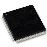
LFXP2-17E-5QN208C8W LATTICE SEMICONDUCTOR, LFXP2-17E-5QN208C8W Datasheet - Page 58

LFXP2-17E-5QN208C8W
Manufacturer Part Number
LFXP2-17E-5QN208C8W
Description
FPGA, 17K LUTS, 146 IO, DSP, 208PQFP
Manufacturer
LATTICE SEMICONDUCTOR
Series
LatticeXP2r
Datasheet
1.LFXP2-5E-5TN144C.pdf
(93 pages)
Specifications of LFXP2-17E-5QN208C8W
No. Of Macrocells
8500
Family Type
LatticeXP2
No. Of Speed Grades
5
No. Of I/o's
146
Clock Management
PLL
Core Supply Voltage Range
1.14V To 1.26V
I/o Supply
RoHS Compliant
- Current page: 58 of 93
- Download datasheet (2Mb)
Lattice Semiconductor
Typical Building Block Function Performance
Pin-to-Pin Performance (LVCMOS25 12mA Drive)
Register-to-Register Performance
Basic Functions
16-bit Decoder
32-bit Decoder
64-bit Decoder
4:1 MUX
8:1 MUX
16:1 MUX
32:1 MUX
Basic Functions
16-bit Decoder
32-bit Decoder
64-bit Decoder
4:1 MUX
8:1 MUX
16:1 MUX
32:1 MUX
8-bit Adder
16-bit Adder
64-bit Adder
16-bit Counter
32-bit Counter
64-bit Counter
64-bit Accumulator
Embedded Memory Functions
512x36 Single Port RAM, EBR Output Registers
1024x18 True-Dual Port RAM (Write Through or Normal, EBR Output Registers)
1024x18 True-Dual Port RAM (Read-Before-Write, EBR Output Registers)
1024x18 True-Dual Port RAM (Write Through or Normal, PLC Output Registers)
Distributed Memory Functions
16x4 Pseudo-Dual Port RAM (One PFU)
32x2 Pseudo-Dual Port RAM
64x1 Pseudo-Dual Port RAM
DSP Functions
18x18 Multiplier (All Registers)
9x9 Multiplier (All Registers)
36x36 Multiply (All Registers)
18x18 Multiply/Accumulate (Input and Output Registers)
18x18 Multiply-Add/Sub-Sum (All Registers)
Function
Function
3-14
1
DC and Switching Characteristics
LatticeXP2 Family Data Sheet
-7 Timing
-7 Timing
521
537
484
744
678
616
529
570
507
293
541
440
321
261
315
315
225
231
760
455
351
365
365
323
281
305
4.4
5.2
5.6
3.7
3.9
4.3
4.5
Units
Units
MHz
MHz
MHz
MHz
MHz
MHz
MHz
MHz
MHz
MHz
MHz
MHz
MHz
MHz
MHz
MHz
MHz
MHz
MHz
MHz
MHz
MHz
MHz
MHz
MHz
MHz
ns
ns
ns
ns
ns
ns
ns
Related parts for LFXP2-17E-5QN208C8W
Image
Part Number
Description
Manufacturer
Datasheet
Request
R

Part Number:
Description:
IC, LATTICEXP2 FPGA, 435MHZ, FPBGA-484
Manufacturer:
LATTICE SEMICONDUCTOR
Datasheet:

Part Number:
Description:
Development Tools & Eval/Demo Boards
Manufacturer:
LATTICE SEMICONDUCTOR
Datasheet:
Part Number:
Description:
FPGA LatticeXP2 Family 17000 Cells Flash Technology 1.2V 484-Pin FBGA
Manufacturer:
LATTICE SEMICONDUCTOR
Datasheet:
Part Number:
Description:
FPGA LatticeXP2 Family 17000 Cells Flash Technology 1.2V 484-Pin FBGA
Manufacturer:
LATTICE SEMICONDUCTOR
Datasheet:
Part Number:
Description:
FPGA LatticeXP2 Family 17000 Cells Flash Technology 1.2V 484-Pin FBGA
Manufacturer:
LATTICE SEMICONDUCTOR
Datasheet:
Part Number:
Description:
Latticexp2 Fpga Data Sheets
Manufacturer:
Lattice Semiconductor Corp.
Datasheet:

Part Number:
Description:
FPGA - Field Programmable Gate Array 5K LUTs 146I/O Inst- on DSP 1.2V -5 Spd
Manufacturer:
Lattice
Datasheet:

Part Number:
Description:
FPGA - Field Programmable Gate Array 5K LUTs 172I/O Inst- on DSP 1.2V -5 Spd
Manufacturer:
Lattice
Datasheet:

Part Number:
Description:
FPGA - Field Programmable Gate Array 5K LUTs 100I/O Inst- on DSP 1.2V -5 Spd
Manufacturer:
Lattice
Datasheet:
Part Number:
Description:
ISPLSI2032-80LT44Lattice Semiconductor [In-System Programmable High Density PLD]
Manufacturer:
Lattice Semiconductor Corp.
Datasheet:
Part Number:
Description:
IC PROGRAMMED LATTICE GAL 16V8
Manufacturer:
Lattice Semiconductor Corp.
Datasheet:
Part Number:
Description:
357-036-542-201 CARDEDGE 36POS DL .156 BLK LOPRO
Manufacturer:
Lattice Semiconductor Corp.
Datasheet:
Part Number:
Description:
357-036-542-201 CARDEDGE 36POS DL .156 BLK LOPRO
Manufacturer:
Lattice Semiconductor Corp.
Datasheet:
Part Number:
Description:
357-036-542-201 CARDEDGE 36POS DL .156 BLK LOPRO
Manufacturer:
Lattice Semiconductor Corp.
Datasheet:
Part Number:
Description:
357-036-542-201 CARDEDGE 36POS DL .156 BLK LOPRO
Manufacturer:
Lattice Semiconductor Corp.
Datasheet:


