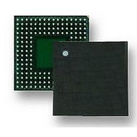
LH7A404N0F000B3 NXP Semiconductors, LH7A404N0F000B3 Datasheet - Page 12

LH7A404N0F000B3
Manufacturer Part Number
LH7A404N0F000B3
Description
MCU ARM9, LCD CTRL, SMD, LFBGA-324
Manufacturer
NXP Semiconductors
Datasheet
1.LH7A404N0F000B3.pdf
(75 pages)
Specifications of LH7A404N0F000B3
Core Size
32bit
No. Of I/o's
64
Ram Memory Size
80KB
Cpu Speed
200MHz
Oscillator Type
External Only
No. Of Timers
3
No. Of Pwm Channels
4
Digital Ic Case Style
LFBGA
Supply Voltage Range
3V
Controller Family/series
LH7A
Peripherals
ADC, DMA, RTC
Rohs Compliant
Yes
Data Bus Width
32 bit
Program Memory Type
ROMLess
Data Ram Size
80 KB
Interface Type
EBI , IrDA , JTAG , PS2 , SCI , UART , USB
Maximum Clock Frequency
200 MHz
Number Of Programmable I/os
64
Number Of Timers
3
Maximum Operating Temperature
+ 85 C
Mounting Style
SMD/SMT
Package / Case
LFBGA
Minimum Operating Temperature
- 40 C
On-chip Adc
10 bit, 9 Channel
Lead Free Status / RoHS Status
Lead free / RoHS Compliant
Available stocks
Company
Part Number
Manufacturer
Quantity
Price
Company:
Part Number:
LH7A404N0F000B3
Manufacturer:
AD
Quantity:
5 742
Company:
Part Number:
LH7A404N0F000B3,55
Manufacturer:
NXP Semiconductors
Quantity:
10 000
LH7A404
NOTES:
1. Signals beginning with ‘n’ are Active LOW.
2. The SCLK pin can source up to 12 mA and sink up to 20 mA.
3. Schmitt trigger input; see ’DC Specifications’, page 31 for triggers
4. These pins have alternate NAND Flash functions during boot-up
5. The nWAIT pin must be pulled HIGH with a 33 kΩ resistor to avoid
6. The internal pullup and pulldown resistance on all digital I/O pins
12
LFBGA
W15
W18
U13
U14
U16
V14
V15
T13
Y14
E12
A11
B11
B10
See ‘DC Characteristics’.
points and hysteresis.
when using the internal Boot ROM. Consult the Boot ROM
Chapter of the User’s Guide for more information.
the possibility of the SMC inadvertently going into WAIT.
is 50K
D6
A3
D5
C4
B3
A2
E5
D3
C2
B1
E3
Ω
AN3/LR/Y-
AN4/WIPER
VSS or VSSA
AN6
AN7
AN8
AN9
SCIO
SCCLK
nSCRESET
SCVCCEN
CTCLKIN
DREQ0
DACK0
DEOT0
DREQ1
DACK1
DEOT1
nTEST0
nTEST1
TDI
TCK
TDO
TMS
.
SIGNAL
• ADC channel 3
• Touch Screen Controller Lower Right
• Touch Screen Controller Y-minus
• ADC channel 4
• Wiper input from 5-wire Touch Screen
Connect pin to either VSS or VSSA
ADC channel 6
ADC channel 7
ADC channel 8
ADC channel 9
Smart Card Interface I/O
Smart Card Interface Clock
Smart Card Interface Reset
Smart Card Interface VCC Enable
Counter Timer Clock Input
DMA Request 0
DMA Acknowledge 0
DMA End of Transfer 0
DMA Request 1
DMA Acknowledge 1
DMA End of Transfer 1
Test Pin 0. Internal weak pull up to VDD. Status
latched at nPOR going HIGH. Pull LOW for JTAG
mode. Pull HIGH (or leave open) for Normal mode.
See Table 3.
Test Pin 1. Internal weak pull up to VDD. Status
latched at nPOR going HIGH. Pull HIGH (or leave
open) for both JTAG and Normal mode. See Table 3.
JTAG Data In. Internal weak pull up to VDD.
JTAG Clock. Internal weak pull up to VDD.
JTAG Data Out
JTAG Test Mode Select. Internal weak pull up to
VDD.
Table 2. LH7A404 Functional Pin List (Cont’d)
DESCRIPTION
NXP Semiconductors
Normal
MODE
JTAG
Input with
Input with
Table 3. nTEST Pin Function
RESET
STATE
pull-up
pull-up
High Z
LOW
LOW
LOW
LOW
Input
Input
Input
Input
Input
Input
Input
Input
Input
Input
Input
Input
Input
Input
Input
Input
Input
nTEST0
No Change
No Change
No Change
No Change
No Change
No Change
No Change
No Change
No Change
No Change
No Change
No Change
STANDBY
0
1
Input with
Input with
STATE
pull-up
pull-up
Input
Input
Input
Input
Input
Input
Input
LOW
LOW
LOW
32-Bit System-on-Chip
Preliminary data sheet
nTEST1
OUTPUT
1
1
DRIVE
12 mA
12 mA
12 mA
12 mA
12 mA
12 mA
12 mA
12 mA
4 mA
nURESET
I/O NOTES
I/O
I/O
I/O
I/O
I/O
I/O
O
O
O
I
I
I
I
I
I
I
I
I
I
I
I
I
I
I
1
x
3


