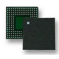
LH7A404N0F000B3 NXP Semiconductors, LH7A404N0F000B3 Datasheet - Page 47

LH7A404N0F000B3
Manufacturer Part Number
LH7A404N0F000B3
Description
MCU ARM9, LCD CTRL, SMD, LFBGA-324
Manufacturer
NXP Semiconductors
Datasheet
1.LH7A404N0F000B3.pdf
(75 pages)
Specifications of LH7A404N0F000B3
Core Size
32bit
No. Of I/o's
64
Ram Memory Size
80KB
Cpu Speed
200MHz
Oscillator Type
External Only
No. Of Timers
3
No. Of Pwm Channels
4
Digital Ic Case Style
LFBGA
Supply Voltage Range
3V
Controller Family/series
LH7A
Peripherals
ADC, DMA, RTC
Rohs Compliant
Yes
Data Bus Width
32 bit
Program Memory Type
ROMLess
Data Ram Size
80 KB
Interface Type
EBI , IrDA , JTAG , PS2 , SCI , UART , USB
Maximum Clock Frequency
200 MHz
Number Of Programmable I/os
64
Number Of Timers
3
Maximum Operating Temperature
+ 85 C
Mounting Style
SMD/SMT
Package / Case
LFBGA
Minimum Operating Temperature
- 40 C
On-chip Adc
10 bit, 9 Channel
Lead Free Status / RoHS Status
Lead free / RoHS Compliant
Available stocks
Company
Part Number
Manufacturer
Quantity
Price
Company:
Part Number:
LH7A404N0F000B3
Manufacturer:
AD
Quantity:
5 742
Company:
Part Number:
LH7A404N0F000B3,55
Manufacturer:
NXP Semiconductors
Quantity:
10 000
32-Bit System-on-Chip
Synchronous Memory Controller Waveforms
chronous Burst Read (page already open). Figure 19
shows the waveform and timing for synchronous mem-
ory to activate a bank and Write.
Preliminary data sheet
NOTES:
1. SDRAMcmd is the combination of nRAS, nCAS, nSDWE, and nSDCSx.
2. tOVXXX represents tOVRA, tOVCA, tOVSDW, or tOVSC.
3. tOHXXX represents tOHRA, tOHCA, tOHSDW, or tOHSC.
4. nDQM is static LOW.
5. SDCKE is static HIGH.
SDRAMcmd
SBANK[1:0]
Figure 18 shows the waveform and timing for a Syn-
SA[13:0],
D[31:0]
SCLK
SSPTXD/
SSPFRM
SSPRXD
SSPCLK
Figure 19. Synchronous Bank Activate and Write
tOVA
t OVXXX
Figure 18. Synchronous Burst Read
MSB
READ
COLUMN
BANK,
t OHXXX
t OVB
NXP Semiconductors
4 to 16 BITS
tISD tIHD
DATA n
DATA n + 1
LSB
DATA n + 2
DATA n + 3
LH7A404-24
LH7A404
LH7A404-13
47


