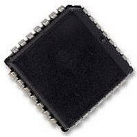
P89LPC936FA NXP Semiconductors, P89LPC936FA Datasheet - Page 52

P89LPC936FA
Manufacturer Part Number
P89LPC936FA
Description
MCU 8BIT 80C51 16K FLASH, PLCC28
Manufacturer
NXP Semiconductors
Datasheet
1.P89LPC936FDH518.pdf
(77 pages)
Specifications of P89LPC936FA
Controller Family/series
(8051) 8052
Core Size
8bit
No. Of I/o's
26
Program Memory Size
16KB
Eeprom Memory Size
512Byte
Ram Memory Size
768Byte
Cpu Speed
18MHz
Oscillator Type
External,
Lead Free Status / RoHS Status
Lead free / RoHS Compliant
Available stocks
Company
Part Number
Manufacturer
Quantity
Price
Company:
Part Number:
P89LPC936FA,529
Manufacturer:
NXP Semiconductors
Quantity:
10 000
Company:
Part Number:
P89LPC936FAЈ¬529
Manufacturer:
NXP
Quantity:
296
NXP Semiconductors
9. A/D converter
P89LPC933_934_935_936
Product data sheet
8.28.10 Hardware activation of the boot loader
8.29 User configuration bytes
8.30 User sector security bytes
9.1 General description
9.2 Features and benefits
The boot loader can also be executed by forcing the device into ISP mode during a
power-on sequence (see the P89LPC933/934/935/936 User manual for specific
information). This has the same effect as having a non-zero status byte. This allows an
application to be built that will normally execute user code but can be manually forced into
ISP operation. If the factory default setting for the boot vector is changed, it will no longer
point to the factory preprogrammed ISP boot loader code. After programming the flash,
the status byte should be programmed to zero in order to allow execution of the user’s
application code beginning at address 0000H.
Some user-configurable features of the P89LPC933/934/935/936 must be defined at
power-up and therefore cannot be set by the program after start of execution. These
features are configured through the use of the flash byte UCFG1. Please see the
P89LPC933/934/935/936 User manual for additional details.
There are eight User Sector Security Bytes on the P89LPC933/934/935/936 device. Each
byte corresponds to one sector. Please see the P89LPC933/934/935/936 User manual for
additional details.
The P89LPC935/936 have two 8-bit, 4-channel multiplexed successive approximation
analog-to-digital converter modules sharing common control logic. The P89LPC933/934
have a single 8-bit, 4-channel multiplexed analog-to-digital converter and an additional
DAC module. A block diagram of the A/D converter is shown in
consists of a 4-input multiplexer which feeds a sample-and-hold circuit providing an input
signal to one of two comparator inputs. The control logic in combination with the SAR
drives a digital-to-analog converter which provides the other input to the comparator. The
output of the comparator is fed to the SAR.
Two (P89LPC935/936) 8-bit, 4-channel multiplexed input, successive approximation
A/D converters with common control logic (one A/D on the P89LPC933/934).
Four result registers for each A/D.
Six operating modes:
Four conversion start modes:
Fixed channel, single conversion mode.
Fixed channel, continuous conversion mode.
Auto scan, single conversion mode.
Auto scan, continuous conversion mode.
Dual channel, continuous conversion mode.
Single step mode.
Timer triggered start.
All information provided in this document is subject to legal disclaimers.
Rev. 8 — 12 January 2011
8-bit microcontroller with accelerated two-clock 80C51 core
P89LPC933/934/935/936
Figure
23. Each A/D
© NXP B.V. 2011. All rights reserved.
52 of 77


