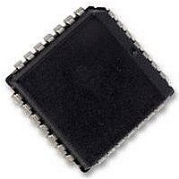
P89LPC936FA NXP Semiconductors, P89LPC936FA Datasheet - Page 55

P89LPC936FA
Manufacturer Part Number
P89LPC936FA
Description
MCU 8BIT 80C51 16K FLASH, PLCC28
Manufacturer
NXP Semiconductors
Datasheet
1.P89LPC936FDH518.pdf
(77 pages)
Specifications of P89LPC936FA
Controller Family/series
(8051) 8052
Core Size
8bit
No. Of I/o's
26
Program Memory Size
16KB
Eeprom Memory Size
512Byte
Ram Memory Size
768Byte
Cpu Speed
18MHz
Oscillator Type
External,
Lead Free Status / RoHS Status
Lead free / RoHS Compliant
Available stocks
Company
Part Number
Manufacturer
Quantity
Price
Company:
Part Number:
P89LPC936FA,529
Manufacturer:
NXP Semiconductors
Quantity:
10 000
Company:
Part Number:
P89LPC936FAЈ¬529
Manufacturer:
NXP
Quantity:
296
NXP Semiconductors
P89LPC933_934_935_936
Product data sheet
9.5.3 Edge triggered
9.5.4 Dual start immediately (P89LPC935/936)
9.6 Boundary limits interrupt
9.7 DAC output to a port pin with high output impedance
9.8 Clock divider
9.9 Power-down and Idle mode
An A/D conversion is started by rising or falling edge of P1.4. Once a conversion has
started, additional edge triggers are ignored until the conversion has completed. The edge
triggered start mode is available in all A/D operating modes.
Programming this mode starts a synchronized conversion of both A/D converters. This
start mode is available in all A/D operating modes. Both A/D converters must be in the
same operating mode. In the continuous conversion modes, both A/D converters must
select an identical number of channels. Any trigger of either A/D will start a simultaneous
conversion of both A/Ds.
Each of the A/D converters has both a high and low boundary limit register. After the four
MSBs have been converted, these four bits are compared with the four MSBs of the
boundary high and low registers. If the four MSBs of the conversion are outside the limit
an interrupt will be generated, if enabled. If the conversion result is within the limits, the
boundary limits will again be compared after all 8 bits have been converted. An interrupt
will be generated, if enabled, if the result is outside the boundary limits. The boundary limit
may be disabled by clearing the boundary limit interrupt enable.
Each A/D converter’s DAC block can be output to a port pin. In this mode, the ADxDAT3
register is used to hold the value fed to the DAC. After a value has been written to the
DAC (written to ADxDAT3), the DAC output will appear on the channel 3 pin.
The A/D converter requires that its internal clock source be in the range of 500 kHz to
3.3 MHz to maintain accuracy. A programmable clock divider that divides the clock
from 1 to 8 is provided for this purpose.
In Idle mode the A/C converter, if enabled, will continue to function and can cause the
device to exit Idle mode when the conversion is completed if the A/D interrupt is enabled.
In Power-down mode or Total Power-down mode, the A/D does not function. If the A/D is
enabled, it will consume power. Power can be reduced by disabling the A/D.
All information provided in this document is subject to legal disclaimers.
Rev. 8 — 12 January 2011
8-bit microcontroller with accelerated two-clock 80C51 core
P89LPC933/934/935/936
© NXP B.V. 2011. All rights reserved.
55 of 77


