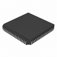
PIC18C801-I/L Microchip Technology, PIC18C801-I/L Datasheet - Page 65

PIC18C801-I/L
Manufacturer Part Number
PIC18C801-I/L
Description
IC,MICROCONTROLLER,8-BIT,PIC CPU,CMOS,LDCC,84PIN,PLASTIC
Manufacturer
Microchip Technology
Series
PIC® 18Cr
Datasheets
1.PIC16F616T-ISL.pdf
(8 pages)
2.PIC18C601-IL.pdf
(320 pages)
3.PIC18C601-IL.pdf
(10 pages)
4.PIC18C601-IL.pdf
(10 pages)
Specifications of PIC18C801-I/L
Rohs Compliant
YES
Core Processor
PIC
Core Size
8-Bit
Speed
25MHz
Connectivity
EBI/EMI, I²C, SPI, UART/USART
Peripherals
Brown-out Detect/Reset, LVD, POR, PWM, WDT
Number Of I /o
37
Program Memory Type
ROMless
Ram Size
1.5K x 8
Voltage - Supply (vcc/vdd)
4.2 V ~ 5.5 V
Data Converters
A/D 12x10b
Oscillator Type
External
Operating Temperature
-40°C ~ 85°C
Package / Case
84-PLCC
Processor Series
PIC18C
Core
PIC
Data Bus Width
8 bit
Data Ram Size
1.5 KB
Interface Type
3-Wire, I2C, SPI, USART
Maximum Clock Frequency
25 MHz
Number Of Programmable I/os
47
Number Of Timers
1 x 16 bit
Operating Supply Voltage
2 V to 5.5 V
Maximum Operating Temperature
+ 85 C
Mounting Style
SMD/SMT
3rd Party Development Tools
52715-96, 52716-328, 52717-734, 52712-325, EWPIC18
Development Tools By Supplier
DV164005, ICE4000, DV164136
Minimum Operating Temperature
- 40 C
On-chip Adc
10 bit
Lead Free Status / RoHS Status
Lead free / RoHS Compliant
For Use With
AC164310 - MODULE SKT FOR PM3 84PLCCXLT84L1 - SOCKET TRANSITION ICE 84PLCCAC174012 - MODULE SKT PROMATEII 84PLCC
Eeprom Size
-
Program Memory Size
-
Lead Free Status / Rohs Status
Details
Other names
PIC18C801-I/LR
PIC18C801-I/LR
PIC18C801I/L
PIC18C801-I/LR
PIC18C801I/L
Available stocks
Company
Part Number
Manufacturer
Quantity
Price
Company:
Part Number:
PIC18C801-I/L
Manufacturer:
MICROCHIP
Quantity:
12 000
Company:
Part Number:
PIC18C801-I/L
Manufacturer:
Microchip Technology
Quantity:
10 000
- PIC16F616T-ISL PDF datasheet
- PIC18C601-IL PDF datasheet #2
- PIC18C601-IL PDF datasheet #3
- PIC18C601-IL PDF datasheet #4
- Current page: 65 of 320
- Download datasheet (6Mb)
FIGURE 5-2:
5.2.2
The 8-bit De-Multiplexed mode applies only to the
PIC18C801. Data and address lines are available sep-
arately. External components are not necessary in this
mode.
For 8-bit De-Multiplexed mode on the PIC18C801, the
instructions are fetched as two 8-bit bytes on a dedi-
cated data bus (PORTJ). The address will be pre-
sented for the entire duration of the fetch cycle on a
separate address bus. The two instruction bytes are
sequentially fetched within one instruction cycle (T
Therefore, the designer must choose external memory
devices according to timing calculations, based on 1/2
T
selection, setup and hold times must be considered.
CY
2001 Microchip Technology Inc.
(2 times instruction rate). For proper memory speed
A16, AD<15:8>
8-BIT DE-MULTIPLEXED MODE
AD<7:0>
ALE
BA0
OE
8-BIT MULTIPLEXED MODE TIMING
Q1
Advance Information
ABh
CY
).
Q2
Opcode Fetch
from 007556h
MOVLW 55h
The Address Latch Enable (ALE) pin is left uncon-
nected, since glue logic is not necessary. The OE out-
put enable signal will enable one byte of program
memory for a portion of the instruction cycle, then BA0
will change and the second byte will be enabled to form
the 16-bit instruction word. The least significant bit of
the address, BA0, must be connected to the memory
devices in this mode. Figure 5-3 shows an example of
8-bit De-Multiplexed mode on the PIC18C801. The
control signals used in 8-bit De-Multiplexed mode are
outlined in Register 5-2. Register 5-4 describes 8-bit
De-Multiplexed mode timing.
03Ah
Q3
55h
PIC18C601/801
Q4
0Eh
DS39541A-page 65
Related parts for PIC18C801-I/L
Image
Part Number
Description
Manufacturer
Datasheet
Request
R

Part Number:
Description:
IC, 8BIT MCU, PIC18F, 40MHZ, LCC-44
Manufacturer:
Microchip Technology
Datasheet:

Part Number:
Description:
IC, 8BIT MCU, PIC18LF, 40MHZ, PLCC-64
Manufacturer:
Microchip Technology
Datasheet:

Part Number:
Description:
IC, 8BIT MCU, PIC18F, 64MHZ, TQFP-80
Manufacturer:
Microchip Technology
Datasheet:

Part Number:
Description:
MCU, MPU & DSP Development Tools CAN/LIN PICtail Plus Daughter Board
Manufacturer:
Microchip Technology
Datasheet:

Part Number:
Description:
IC, 8BIT MCU, PIC18F, 64MHZ, DIP-40
Manufacturer:
Microchip Technology
Datasheet:

Part Number:
Description:
IC, 8BIT MCU, PIC18LF, 40MHZ, PLCC-64
Manufacturer:
Microchip Technology
Datasheet:

Part Number:
Description:
IC, 8BIT MCU, PIC18F, 64MHZ, TQFP-64
Manufacturer:
Microchip Technology

Part Number:
Description:
IC, 8BIT MCU, PIC18F, 64MHZ, TQFP-80
Manufacturer:
Microchip Technology

Part Number:
Description:
8KB, Flash, 768bytes-RAM, 36I/O, 8-bit Family,nanowatt XLP 40 UQFN 5x5x0.5mm TUB
Manufacturer:
Microchip Technology
Datasheet:

Part Number:
Description:
8KB, Flash, 768bytes-RAM, 36I/O, 8-bit Family,nanowatt XLP 40 UQFN 5x5x0.5mm TUB
Manufacturer:
Microchip Technology

Part Number:
Description:
16KB, Flash, 768bytes-RAM, 36I/O, 8-bit Family,nanowatt XLP 40 UQFN 5x5x0.5mm TU
Manufacturer:
Microchip Technology
Datasheet:

Part Number:
Description:
16KB, Flash, 768bytes-RAM, 36I/O, 8-bit Family,nanowatt XLP 40 UQFN 5x5x0.5mm TU
Manufacturer:
Microchip Technology

Part Number:
Description:
32KB, Flash, 1536bytes-RAM, 36I/O, 8-bit Family,nanowatt XLP 40 UQFN 5x5x0.5mm T
Manufacturer:
Microchip Technology
Datasheet:

Part Number:
Description:
32KB, Flash, 1536bytes-RAM, 36I/O, 8-bit Family,nanowatt XLP 40 UQFN 5x5x0.5mm T
Manufacturer:
Microchip Technology

Part Number:
Description:
64KB, Flash, 3968bytes-RAM, 36I/O, 8-bit Family,nanowatt XLP 40 UQFN 5x5x0.5mm T
Manufacturer:
Microchip Technology
Datasheet:


