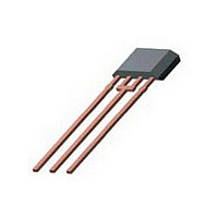
A1373LKB Allegro Microsystems Inc, A1373LKB Datasheet
A1373LKB
Specifications of A1373LKB


Related parts for A1373LKB


A1373LKB Summary of contents
Page 1
These parts are in production but have been determined to be NOT FOR NEW DESIGN. This classification indicates that sale of this device is currently restricted to existing customer applications. The device should not be purchased for new design applications ...
Page 2
Features and Benefits ▪ Output pin programming ▪ Field-programmable for optimal application integration ▪ Selectable coarse and fine gain and quiescent output voltage ▪ Selectable sensitivity temperature coefficient ▪ Selectable output clamp voltage level, including no-clamp (rail-to-rail) ▪ Selectable output ...
Page 3
... In this manner, manufacturing tolerances can be reduced and the assembly process can be simplified. Selection Guide Part Number A1373EKB–T Bulk, 500 pieces / bag A1373LKB–T Bulk, 500 pieces / bag A1374EKB–T Bulk, 500 pieces / bag A1374LKB–T Bulk, 500 pieces / bag * Contact Allegro for additional packing options ...
Page 4
A1373 and A1374 CHARACTERISTIC PARAMETERS Characteristic over operating temperature range, V ELECTRICAL CHARACTERISTICS Supply Voltage Supply Current Reverse-Supply Current Power-On Time 1 Chopping Frequency Internal Bandwidth over operating temperature range, V OUTPUT CHARACTERISTICS Noise 2,3 Output Capacitance Load Output Resistive ...
Page 5
A1373 and A1374 CHARACTERISTIC PARAMETERS (continued) Characteristic QUIESCENT OUTPUT VOLTAGE PROGRAMMING Quiescent Output Voltage Range Average Quiescent Output Voltage Step Size 4,5,6 Quiescent Output Voltage Err Programming Resolution Quiescent Output Voltage Drift Over Operating Temperature Range Quiescent Output Voltage Programming ...
Page 6
A1373 and A1374 CHARACTERISTIC PARAMETERS (continued) Characteristic SENSITIVITY TEMPERATURE COEFFICIENT PROGRAMMING otherwise noted Sensitivity Temperature Coefficient Range Average Sensitivity Temperature Coefficient Step Size Sensitivity Temperature Coefficient Programming Bits ONE-TIME PROGRAMMING Device Programming Lock Bit RATIOMETRY over ...
Page 7
A1373 and A1374 3.4 3.2 Positive Programming Codes 3.0 2.8 2.6 2.4 2.2 2 High Precision, Output Pin Programmable Linear Hall Effect Sensor ICs Typical Characteristics Temperature Coefficient Code Profile T = 150°C, Magnetically Back-Biased ...
Page 8
A1373 and A1374 Sensitivity Temperature Coefficient Range, TC 0.25 0.20 0.15 Extended Range Not Guaranteed 0.10 0.05 Guaranteed Programmable Range 0 –0.05 Extended Range Not Guaranteed –0.10 –0.15 A Units with the range TC –0.20 before programming ...
Page 9
A1373 and A1374 Average Ratiometry, Voq 101.0 100.8 4.5 to 5.0 V 100.6 5.5 to 5.0 V 100.4 100.2 100.0 99.8 99.6 99.4 99.2 99.0 -50 - Temperature (°C) Average Symmetry vs Temperature 101.0 100.8 100.6 100.4 ...
Page 10
A1373 and A1374 Average Delta Sensitivity (percent change relative to 25°C) 8 Sensitivity Low 6 Sensitivity Mid Sensitivity High -50 - Temperature (°C) Average Delta Sensitivity (percent per degree Celsius change ...
Page 11
A1373 and A1374 Average Quiescent Output Voltage 3.5 3.0 Vout(q)Low - Initial 2.5 Vout(q)Mid - Initial Vout(q)High - Initial 2.0 1.5 1.0 0.5 0 -50 - Temperature (°C) Average Quiescent Output Voltage Max Code (511 ...
Page 12
A1373 and A1374 Average Saturation Voltage -50 - Temperature (°C) High Precision, Output Pin Programmable Linear Hall Effect Sensor ICs OUT(sat OUT(sat)– -50 ...
Page 13
A1373 and A1374 Chopper Stabilization Technique Chopper stabilization is a unique approach used to minimize Hall offset on the chip. The patented Allegro technique, namely Dynamic Quadrature Offset Cancellation, removes key sources of the output drift induced by thermal and ...
Page 14
A1373 and A1374 A type of Hall-Effect device that produces an analog output Linear: voltage proportional to the strength of a sensed magnetic field. Ratiometric: A linear Hall-Effect device that, when not subjected to a significant magnetic field, has an ...
Page 15
A1373 and A1374 Quiescent Output Voltage. In the quiescent state (no signifi- cant magnetic field 0), the output, V the supply voltage throughout the entire operating ranges and ambient temperature Due ...
Page 16
A1373 and A1374 Several parameters can be field-programmed so, a coded series of voltage pulses through the VOUT pin is used to set bitfields in onboard registers. The effect on the device output can be monitored, and the ...
Page 17
A1373 and A1374 The mid voltage range neutral level used to separate PM V and V pulses from each other The low level pulse is used to increment the mode, register, PL ...
Page 18
A1373 and A1374 QVO V PL Coarse High Precision, Output Pin Programmable Linear Hall Effect Sensor ICs Programming State Machine POWER UP INITIAL STATE V PH MODE SELECT V PL TRY V BLOW V ...
Page 19
A1373 and A1374 Programming Protocol and State Machine Description INITIAL STATE After system power-up, the programming logic is reset to a known state. This is referred to as the Initial state. All the regis- ters that have intact fuses are ...
Page 20
A1373 and A1374 Binary Bitfield Address QVO Coarse register QVO Fine register 000000000 111111111 Sens. Coarse register Sens. Fine register 00000000 11111111 TC Register register (See also chart Sensitivity Temperature Coefficient Code ...
Page 21
A1373 and A1374 • A bypass capacitor rated at 0.1μF must be mounted between the VOUT pin and the GND pin during programming. The power supply used for programming should be capable of delivering 28 V and 300 mA. • ...
Page 22
A1373 and A1374 This example demonstrates the programming of the devices by setting the register for Sensitivity Temperature Coefficient to 00110. 1. Power-on the system. This will reset the unprogrammed bits in all registers to 0. The device enters the ...
Page 23
A1373 and A1374 5.21 45° +0.08 3.43 –0.05 2.16 MAX 14.73 ±0.51 +0.07 0.51 –0. Terminal List Name VCC GND VOUT Copyright ©2005-2008, Allegro MicroSystems, Inc. Allegro MicroSystems, Inc. reserves the right to make, from time to time, ...