A1373LKB Allegro Microsystems Inc, A1373LKB Datasheet - Page 17
A1373LKB
Manufacturer Part Number
A1373LKB
Description
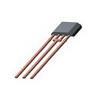
IC SENSOR HALL EFFECT PREC 3-SIP
Manufacturer
Allegro Microsystems Inc
Type
Bipolar or Unipolar, Programmabler
Datasheet
1.A1374LKB-T.pdf
(23 pages)
Specifications of A1373LKB
Sensing Range
1.75mV/G ~ 11.25mV/G
Voltage - Supply
4.5 V ~ 5.5 V
Current - Supply
10mA
Current - Output (max)
10mA
Output Type
Analog, Ratiometric
Features
High Precision
Operating Temperature
-40°C ~ 150°C
Package / Case
3-SIP
Magnetic Type
Unipolar
Operating Supply Voltage (min)
4.5V
Operating Supply Voltage (typ)
5V
Operating Supply Voltage (max)
5.5V
Output Current
10mA
Package Type
SIP
Pin Count
3
Mounting
Through Hole
Operating Temp Range
-40C to 150C
Operating Temperature Classification
Automotive
Lead Free Status / RoHS Status
Contains lead / RoHS non-compliant


A1373
A1374
The mid voltage range, V
V
The low level, V
and bitfield addresses that are to be set. The device generates a
V
tion, V
In Try Value mode,the programming drive signal can be held
at 5 V or less if no code search is required. If a code search is
PH
PL
30
25
20
15
10
30
25
20
15
10
5
0
5
0
Try Mode
pulse on the falling edge of the mid-level to low-level transi-
and V
selected
A. Try Value Mode. Code search with drive signal held
at 5 V.
C. Blow Fuse Mode: Code 8 / bit 4 is programmed.
Mode Select
(Code 1)
PM
t
Mode Select
PHE
(Code 2)
t
PME
Blow
Fuse
mode
selected
to V
1
PL
1
and
pulses from each other.
2
Register Select
PL
t
PLA
1
(Code 3)
PL
.
Register Select
Sensitivity
Fine
register
selected
2
(Qvo Fine)
1
, pulse is used to increment the mode, register,
(Code 3)
t
PMA
(Sensitivity Coarse)
3
2
Sensitivity Fine selected
3
PM
1
, is a neutral level used to separate
1
2
Time (μs)
= Programming edge
2
Time (μs)
3
Bitfield Select
Bitfield Select
3
4
(Code 10)
(Code 8)
4
5
5
6
Bitfield 8
address
selected
6
7
10th address
selected
8
7
High Precision, Output Pin Programmable
9
8
10
Blow Fuse
Try Mode
selected
Mode Select
(Code 1)
1
}
}
}
}
V
V
V
V
V
V
PH
PM
PL
PH
PM
PL
required, then the output drive signal must be released to allow
the output level to be read for each bitfield increment (see panels
A and B, below).
To guarantee proper pulse recognition, each level must be held
for the predefined durations specified in the Programming Proto-
col Characteristics table. Failure to follow the specifications may
produce undefined results. Examples of common pulse trains are
shown in panels C and D, below.
30
25
20
15
10
30
25
20
15
10
5
0
5
0
B. Try Value Mode. Code search with drive signal released
after each V
increment.
D. Lock Device Mode. Device-level Lock Bit is programmed;
device programming is then permanently disabled.
2.0
Mode Select
Linear Hall Effect Sensor ICs
(Code 1)
t
PHE
1
t
V
V
PME
Mode Select
OUT
OUT
(Code 3)
Register Select
1
1
measurements
measurements
(Code 3)
PM
2
, allows output to be measured after each code
t
PLA
2
3
Lock
Device
mode
selected
t
PMA
Register Select
(Code 0)
2.1
3
1
Removing the output drive signal after each
V
PM
115 Northeast Cutoff
1.508.853.5000; www.allegromicro.com
2.2
Allegro MicroSystems, Inc.
Worcester, Massachusetts 01615-0036 U.S.A.
2
allows measurement of the output pin
Time (us)
2.3
Time (μs)
3
Bitfield Select
(Code 1)
2.4
Holding at V
Holding at V
V
V
will increment by 1 bitfield
will increment by 1 bitfield
Bitfield Select
4
(Code 10)
PL
PL
2.5
is required; dropping to V
is required; dropping to V
5
1
2.6
6
PM
PM
Lock (blow Lock Bit fuse)
2.7
is allowed when no
is allowed when no
t
7
PHP
2.8
8
2.9
9
PL
PL
3.0
10
1
Mode Select
(Code 1)
2.0
1
}
}
}
}
V
V
V
V
V
V
16
PH
PM
PL
PH
PM
PL
Related parts for A1373LKB
Image
Part Number
Description
Manufacturer
Datasheet
Request
R

Part Number:
Description:
IC, HALL EFFECT SENSOR, Linear, SOIC-8
Manufacturer:
Allegro Microsystems Inc
Datasheet:
Part Number:
Description:
IC, HALL EFFECT SENSOR, Linear, SOIC-8
Manufacturer:
Allegro Microsystems Inc
Datasheet:
Part Number:
Description:
IC, HALL EFFECT SENSOR, Linear, SOIC-8
Manufacturer:
Allegro Microsystems Inc
Datasheet:

Part Number:
Description:
IC SWITCH INTERFACE 2CHAN 8-SOIC
Manufacturer:
Allegro Microsystems Inc
Datasheet:

Part Number:
Description:
IC SMOKE DETECTOR ION 16-DIP
Manufacturer:
Allegro Microsystems Inc
Datasheet:
Part Number:
Description:
IC SMOKE DETECTOR ION 16-DIP
Manufacturer:
Allegro Microsystems Inc
Datasheet:
Part Number:
Description:
IC SMOKE DETECTOR ION 16-DIP
Manufacturer:
Allegro Microsystems Inc
Datasheet:
Part Number:
Description:
IC SMOKE DETECTOR PHOTO 16-DIP
Manufacturer:
Allegro Microsystems Inc
Datasheet:
Part Number:
Description:
IC SMOKE DETECTOR ION 16-DIP
Manufacturer:
Allegro Microsystems Inc
Datasheet:
Part Number:
Description:
IC SMOKE DETECTOR PHOTO 16-DIP
Manufacturer:
Allegro Microsystems Inc
Datasheet:
Part Number:
Description:
IC SMOKE DETECTOR PHOTO 16-DIP
Manufacturer:
Allegro Microsystems Inc
Datasheet:
Part Number:
Description:
IC SMOKE DETECTOR ION 16-DIP
Manufacturer:
Allegro Microsystems Inc
Datasheet:
Part Number:
Description:
IC SMOKE DETECTOR PHOTO 16-SOIC
Manufacturer:
Allegro Microsystems Inc
Datasheet:

Part Number:
Description:
IC LED DRIVER HIGH BRIGHT 16-QFN
Manufacturer:
Allegro Microsystems Inc
Datasheet:

Part Number:
Description:
IC LED DRIVER AUTOMOTIVE 8-SOIC
Manufacturer:
Allegro Microsystems Inc
Datasheet: