SI8401DB-T1-E1 Vishay, SI8401DB-T1-E1 Datasheet - Page 6
SI8401DB-T1-E1
Manufacturer Part Number
SI8401DB-T1-E1
Description
P CH MOSFET, -20V, 4.9A, MICRO FOOT
Manufacturer
Vishay
Series
TrenchFET®r
Specifications of SI8401DB-T1-E1
Transistor Polarity
P Channel
Continuous Drain Current Id
-4.9A
Drain Source Voltage Vds
-20V
On Resistance Rds(on)
95mohm
Rds(on) Test Voltage Vgs
12V
Threshold Voltage Vgs Typ
1.4V
Fet Type
MOSFET P-Channel, Metal Oxide
Fet Feature
Logic Level Gate
Rds On (max) @ Id, Vgs
65 mOhm @ 1A, 4.5V
Drain To Source Voltage (vdss)
20V
Current - Continuous Drain (id) @ 25° C
3.6A
Vgs(th) (max) @ Id
1.4V @ 250µA
Gate Charge (qg) @ Vgs
17nC @ 4.5V
Power - Max
1.47W
Mounting Type
Surface Mount
Package / Case
4-MICRO FOOT®CSP
Lead Free Status / RoHS Status
Lead free / RoHS Compliant
Other names
SI8401DB-T1-E1TR
Available stocks
Company
Part Number
Manufacturer
Quantity
Price

Part Number:
SI8401DB-T1-E1
Manufacturer:
VISHAY/威世
Quantity:
20 000


Johnson Zhao
INTRODUCTION
Vishay Siliconix’s MICRO FOOT product family is based on a
wafer-level chip-scale packaging (WL-CSP) technology that
implements a solder bump process to eliminate the need for an
outer package to encase the silicon die. MICRO FOOT
products include power MOSFETs, analog switches, and
power ICs.
For battery powered compact devices, this new packaging
technology reduces board space requirements, improves
thermal performance, and mitigates the parasitic effect typical
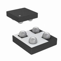
of leaded packaged products. For example, the 6−bump
MICRO FOOT Si8902EDB common drain power MOSFET,
which measures just 1.6 mm x 2.4 mm, achieves the same
performance as TSSOP−8 devices in a footprint that is 80%
smaller and with a 50% lower height profile (Figure 1). A
MICRO FOOT analog switch, the 6−bump DG3000DB, offers
low charge injection and 1.4 W on−resistance in a footprint
measuring just 1.08 mm x 1.58 mm (Figure 2).
Vishay Siliconix MICRO FOOT products can be handled with
the same process techniques used for high-volume assembly
of packaged surface-mount devices. With proper attention to
PCB and stencil design, the device will achieve reliable
performance without underfill. The advantage of the device’s
small footprint and short thermal path make it an ideal option
for space-constrained applications in portable devices such as
battery packs, PDAs, cellular phones, and notebook
computers.
This application note discusses the mechanical design and
reliability of MICRO FOOT, and then provides guidelines for
board layout, the assembly process, and the PCB rework
process.
Document Number: 71990
06-Jan-03
PCB Design and Assembly Guidelines
For MICRO FOOTr Products
FIGURE 1. 3D View of MICRO FOOT Products Si8902DB and
0.18 ~ 0.25
0.285
0.5
FIGURE 2. Outline of MICRO FOOT CSP & Analog
Si8900EDB
0.285
Switch DG3000DB
3
0.5
1.58
2
Vishay Siliconix
1
www.vishay.com
AN824
A
B
1.08
1
Related parts for SI8401DB-T1-E1
Image
Part Number
Description
Manufacturer
Datasheet
Request
R


Part Number:
Description:
P-Channel 20-V (D-S) MOSFET
Manufacturer:
VISHAY [Vishay Siliconix]
Datasheet:

Part Number:
Description:
P-channel 20-v D-s Mosfet
Manufacturer:
Vishay
Datasheet:

Part Number:
Description:
357-036-542-201 CARDEDGE 36POS DL .156 BLK LOPRO
Manufacturer:
Vishay
Datasheet:
Part Number:
Description:
357-036-542-201 CARDEDGE 36POS DL .156 BLK LOPRO
Manufacturer:
Vishay
Datasheet:
Part Number:
Description:
357-036-542-201 CARDEDGE 36POS DL .156 BLK LOPRO
Manufacturer:
Vishay
Datasheet:
Part Number:
Description:
357-036-542-201 CARDEDGE 36POS DL .156 BLK LOPRO
Manufacturer:
Vishay
Datasheet:
Part Number:
Description:
357-036-542-201 CARDEDGE 36POS DL .156 BLK LOPRO
Manufacturer:
Vishay
Datasheet:
Part Number:
Description:
357-036-542-201 CARDEDGE 36POS DL .156 BLK LOPRO
Manufacturer:
Vishay
Datasheet:
Part Number:
Description:
357-036-542-201 CARDEDGE 36POS DL .156 BLK LOPRO
Manufacturer:
Vishay
Datasheet:
Part Number:
Description:
357-036-542-201 CARDEDGE 36POS DL .156 BLK LOPRO
Manufacturer:
Vishay
Datasheet:
Part Number:
Description:
357-036-542-201 CARDEDGE 36POS DL .156 BLK LOPRO
Manufacturer:
Vishay
Datasheet:
Part Number:
Description:
357-036-542-201 CARDEDGE 36POS DL .156 BLK LOPRO
Manufacturer:
Vishay
Datasheet: