SI8401DB-T1-E1 Vishay, SI8401DB-T1-E1 Datasheet - Page 8
SI8401DB-T1-E1
Manufacturer Part Number
SI8401DB-T1-E1
Description
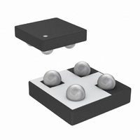
P CH MOSFET, -20V, 4.9A, MICRO FOOT
Manufacturer
Vishay
Series
TrenchFET®r
Specifications of SI8401DB-T1-E1
Transistor Polarity
P Channel
Continuous Drain Current Id
-4.9A
Drain Source Voltage Vds
-20V
On Resistance Rds(on)
95mohm
Rds(on) Test Voltage Vgs
12V
Threshold Voltage Vgs Typ
1.4V
Fet Type
MOSFET P-Channel, Metal Oxide
Fet Feature
Logic Level Gate
Rds On (max) @ Id, Vgs
65 mOhm @ 1A, 4.5V
Drain To Source Voltage (vdss)
20V
Current - Continuous Drain (id) @ 25° C
3.6A
Vgs(th) (max) @ Id
1.4V @ 250µA
Gate Charge (qg) @ Vgs
17nC @ 4.5V
Power - Max
1.47W
Mounting Type
Surface Mount
Package / Case
4-MICRO FOOT®CSP
Lead Free Status / RoHS Status
Lead free / RoHS Compliant
Other names
SI8401DB-T1-E1TR
Available stocks
Company
Part Number
Manufacturer
Quantity
Price

Part Number:
SI8401DB-T1-E1
Manufacturer:
VISHAY/威世
Quantity:
20 000


Á Á Á
Á Á Á
Á Á Á
Á Á Á
Á Á Á
Á Á Á
Á Á Á
Board pad design. The landing-pad size for MICRO FOOT
products is determined by the bump pitch as shown in Table 3.
The pad pattern is circular to ensure a symmetric,
barrel-shaped solder bump.
ASSEMBLY PROCESS
MICRO FOOT products’ surface-mount-assembly operations
include solder paste printing, component placement, and
solder reflow as shown in the process flow chart (Figure 5).
Stencil design. Stencil design is the key to ensuring
maximum solder paste deposition without compromising the
assembly yield from solder joint defects (such as bridging and
extraneous solder spheres). The stencil aperture is dependent
on the copper pad size, the solder mask opening, and the
quantity of solder paste.
In MICRO FOOT products, the stencil is 0.125-mm (5-mils)
thick. The recommended apertures are shown in Table 3 and
are fabricated by laser cut.
Solder-paste printing. The solder-paste printing process
involves transferring solder paste through pre-defined
apertures via application of pressure.
In MICRO FOOT products, the solder paste used is UP78
No-clean eutectic 63 Sn/37Pb type3 or finer solder paste.
Document Number: 71990
06-Jan-03
0.80 mm
0.50 mm
Pitch
Dimensions of Copper Pad and Solder Mask
Á Á Á Á Á
Á Á Á Á Á
Á Á Á Á Á
Á Á Á Á Á
Á Á Á Á Á
Á Á Á Á Á
Á Á Á Á Á
Opening in PCB and Stencil Aperture
Copper Pad
0.30 " 0.01 mm
0.17 " 0.01 mm
FIGURE 5. SMT Assembly Process Flow
IIncoming Tape and Reel Inspection
Solder Joint Inspection
Solder Paste Printing
Á Á Á Á Á
Á Á Á Á Á
Á Á Á Á Á
Á Á Á Á Á
Á Á Á Á Á
Á Á Á Á Á
Á Á Á Á Á
TABLE 3
Chip Placement
Pack and Ship
Stencil Design
Solder Mask
0.41 " 0.01 mm
0.27 " 0.01 mm
Opening
Reflow
Á Á Á Á Á
Á Á Á Á Á
Á Á Á Á Á
Á Á Á Á Á
Á Á Á Á Á
Á Á Á Á Á
Á Á Á Á Á
in square aperture
in ciircle aperture
0.33 " 0.01 mm
0.30 " 0.01 mm
Aperture
Stencil
Chip pick-and-placement. MICRO FOOT products can be
picked and placed with standard pick-and-place equipment.
The recommended pick-and-place force is 150 g. Though the
part will self-center during solder reflow, the maximum
placement offset is 0.02 mm.
Reflow Process. MICRO FOOT products can be assembled
using standard SMT reflow processes. Similar to any other
package, the thermal profile at specific board locations must
be determined. Nitrogen purge is recommended during reflow
operation. Figure 6 shows a typical reflow profile.
PCB REWORK
To replace MICRO FOOT products on PCB, the rework
procedure is much like the rework process for a standard BGA
or CSP, as long as the rework process duplicates the original
reflow profile. The key steps are as follows:
1.
2.
3.
4.
5.
6.
Apply gel flux to the pad.
Remove the MICRO FOOT device using a convection
nozzle to create localized heating similar to the original
reflow profile. Preheat from the bottom.
Once the nozzle temperature is +190_C, use tweezers to
remove the part to be replaced.
Resurface the pads using a temperature-controlled
soldering iron.
Use a vacuum needle pick-up tip to pick up the
replacement part, and use a placement jig to placed it
accurately.
Reflow the part using the same convection nozzle, and
preheat from the bottom, matching the original reflow
profile.
250
200
150
100
50
0
0
FIGURE 6. Reflow Profile
100
Thermal Profile
Time (Seconds
200
Vishay Siliconix
300
www.vishay.com
AN824
400
3
Related parts for SI8401DB-T1-E1
Image
Part Number
Description
Manufacturer
Datasheet
Request
R


Part Number:
Description:
P-Channel 20-V (D-S) MOSFET
Manufacturer:
VISHAY [Vishay Siliconix]
Datasheet:

Part Number:
Description:
P-channel 20-v D-s Mosfet
Manufacturer:
Vishay
Datasheet:

Part Number:
Description:
357-036-542-201 CARDEDGE 36POS DL .156 BLK LOPRO
Manufacturer:
Vishay
Datasheet:
Part Number:
Description:
357-036-542-201 CARDEDGE 36POS DL .156 BLK LOPRO
Manufacturer:
Vishay
Datasheet:
Part Number:
Description:
357-036-542-201 CARDEDGE 36POS DL .156 BLK LOPRO
Manufacturer:
Vishay
Datasheet:
Part Number:
Description:
357-036-542-201 CARDEDGE 36POS DL .156 BLK LOPRO
Manufacturer:
Vishay
Datasheet:
Part Number:
Description:
357-036-542-201 CARDEDGE 36POS DL .156 BLK LOPRO
Manufacturer:
Vishay
Datasheet:
Part Number:
Description:
357-036-542-201 CARDEDGE 36POS DL .156 BLK LOPRO
Manufacturer:
Vishay
Datasheet:
Part Number:
Description:
357-036-542-201 CARDEDGE 36POS DL .156 BLK LOPRO
Manufacturer:
Vishay
Datasheet:
Part Number:
Description:
357-036-542-201 CARDEDGE 36POS DL .156 BLK LOPRO
Manufacturer:
Vishay
Datasheet:
Part Number:
Description:
357-036-542-201 CARDEDGE 36POS DL .156 BLK LOPRO
Manufacturer:
Vishay
Datasheet:
Part Number:
Description:
357-036-542-201 CARDEDGE 36POS DL .156 BLK LOPRO
Manufacturer:
Vishay
Datasheet: