HDLO-3416 Avago Technologies US Inc., HDLO-3416 Datasheet - Page 11
HDLO-3416
Manufacturer Part Number
HDLO-3416
Description
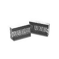
DISPLAY DOT MATRIX 32.77X20.07MM 5X7 RED
Manufacturer
Avago Technologies US Inc.
Series
HDLx-3416r
Datasheet
1.HDLO-3416.pdf
(12 pages)
Specifications of HDLO-3416
Character Format
Dot Matrix
Character Size
6.9mm
Led Color
Red
Luminous Intensity
3.5mcd
No. Of Digits / Alpha
4
Display Area Width
32.77mm
Display Area Height
10.16mm
Millicandela Rating
*
Internal Connection
*
Size / Dimension
1.29" x 0.79" (32.77mm x 20.07mm)
Color
Red
Configuration
*
Voltage - Forward (vf) Typ
*
Package / Case
22-DIP
Display Type
Alphanumeric
Number Of Digits/alpha
4
Digit/alpha Size
0.27" (6.86mm)
Number Of Digits
4
Illumination Color
Red
Wavelength
626 nm
Operating Voltage
- 0.5 V to 7 V
Maximum Operating Temperature
+ 85 C
Minimum Operating Temperature
- 40 C
Lead Free Status / RoHS Status
Lead free / RoHS Compliant
Common Pin
-
Lead Free Status / Rohs Status
Details


+ V
250 k
Figure 4. Intensity modulation control using
an astable multivibrator (reprinted with
permission from Electronics magazine, Sept.
19, 1974, VNU Business pub. Inc.).
11
Figure 4 shows a circuit
designed to dim the display from
98% to 2% by pulse width
modulating the BL input. A
logarithmic or a linear
potentiometer may be used to
adjust the display intensity.
However, a logarithmic potentio-
meter matches the response of
the human eye and therefore
provides better resolution at low
intensities. The circuit
frequency should be designed to
operate at 10 kHz or higher.
Lower frequencies may cause
the display to flicker.
Extended Function Disable
Extended Function Disable (bit
D
disables the extended blanking
and dimming functions in the
HDLX-3416. If the Extended
Function Disable is a logic 1, the
internal brightness control,
Master Blank, and Digit Blank
Disable bits are ignored.
However, the BL input and
Cursor control are still active.
LOG
6
DD
of the Control Register)
1 k
1N914
400 pF
1 k
7
6
8
2
555
1
4
3
BL
(PIN 18)
10 kHz
OUTPUT
Mechanical and Electrical
Considerations
The HDLX-3416 is a 22 pin DIP
package that can be stacked
horizontally and vertically to
create arrays of any size. The
display is designed to operate
continuously from -40 C to
+85 C for all possible input
conditions.
The HDLX-3416 is assembled by
die attaching and wire bonding
140 LEDs and a CMOS IC to a
high temperature printed circuit
board. A polycarbonate lens is
placed over the PC board
creating an air gap environment
for the LED wire bonds. Backfill
epoxy environmentally seals the
display package. This package
construction makes the display
highly tolerant to temperature
cycling and allows wave
soldering.
The inputs to the CMOS IC are
protected against static
discharge and input current
latchup. However, for best
results standard CMOS handling
precautions should be used.
Prior to use, the HDLX-3416
should be stored in anti-static
tubes or conductive material.
During assembly a grounded
conductive work area should be
used, and assembly personnel
should wear conductive wrist
straps. Lab coats made of
synthetic material should be
avoided since they are prone to
static charge build-up.
Input current latchup is caused
when the CMOS inputs are sub-
jected either to a voltage below
ground (Vin < ground) or to a
voltage higher than V
V
forced into the input. To prevent
input current latchup and ESD
damage, unused inputs should
DD
) and when a high current is
DD
(Vin >
be connected either to ground or
to V
applied to the inputs until V
has been applied to the display.
Transient input voltages should
be eliminated.
Soldering and Post Solder Cleaning
Instructions for the HDLX-3416
The HDLX-3416 may be hand
soldered or wave soldered with
SN63 solder. When hand solder-
ing it is recommended that an
electronically temperature con-
trolled and securely grounded
soldering iron be used. For best
results, the iron tip temperature
should be set at 315 C (600 F).
For wave soldering, a rosin-
based RMA flux can be used. The
solder wave temperature should
be set at 245 C
(473 F
wave should be set between 1
to 3 seconds for optimum
soldering. The preheat
temperature should not exceed
110 C (230 F) as measured on
the solder side of the PC board.
For further information on
soldering and post solder
cleaning, see Application Note
1027, Soldering LED
Components.
Contrast Enhancement
The objective of contrast
enhancement is to provide good
readability in the end user’s
ambient lighting conditions. The
concept is to employ both
luminance and chrominance
contrast techniques. These
enhance readability by having
the OFF-dots blend into the
display background and the ON-
dots vividly stand out against
the same background. For addi-
tional information on contrast
enhancement, see Application
Note 1015.
DD
. Voltages should not be
9 F), and dwell in the
5 C
DD
1
/
2
Related parts for HDLO-3416
Image
Part Number
Description
Manufacturer
Datasheet
Request
R

Part Number:
Description:
LED DISPLAY 5X7 5MM 4CHAR HE RED
Manufacturer:
Avago Technologies US Inc.
Datasheet:

Part Number:
Description:
DISPLAY 5X7 0.15" 4CHAR RED
Manufacturer:
Avago Technologies US Inc.
Datasheet:

Part Number:
Description:
DISPLAY DOT MATRIX 25.15X20.07MM 5X7 RED
Manufacturer:
Avago Technologies US Inc.
Datasheet:

Part Number:
Description:
OPTOCOUPLER GATE DRV 2A 16-SOIC
Manufacturer:
Avago Technologies US Inc.
Datasheet:
Part Number:
Description:
OPTOCOUPLER 2CH 2.5A 16-SOIC
Manufacturer:
Avago Technologies US Inc.
Datasheet:

Part Number:
Description:
OPTOCOUPLER GATE DRV 0.4A 16SOIC
Manufacturer:
Avago Technologies US Inc.
Datasheet:

Part Number:
Description:
OPTOCOUPLER 2.0A 250KHZ 8-DIP
Manufacturer:
Avago Technologies US Inc.
Datasheet:

Part Number:
Description:
OPTOCOUPLER 2.0A 250KHZ GW 8-SMD
Manufacturer:
Avago Technologies US Inc.
Datasheet:

Part Number:
Description:
OPTOCOUPLER 2CH 15MBD 3.3V 8SOIC
Manufacturer:
Avago Technologies US Inc.
Datasheet:
Part Number:
Description:
OPTOCOUPLER DARL-OUT 8-DIP
Manufacturer:
Avago Technologies US Inc.
Datasheet:
Part Number:
Description:
OPTOCOUPLER IGBT DRIVE 0.4A 8DIP
Manufacturer:
Avago Technologies US Inc.
Datasheet:
Part Number:
Description:
OPTOCOUPLER DARL-OUT 8-DIP
Manufacturer:
Avago Technologies US Inc.
Datasheet:

Part Number:
Description:
OPTOCOUPLER 1CH 1MBS 8-SMD GW
Manufacturer:
Avago Technologies US Inc.
Datasheet:
Part Number:
Description:
OPTOCOUPLER GATE DRIVER 8-DIP
Manufacturer:
Avago Technologies US Inc.
Datasheet:

Part Number:
Description:
OPTOCOUPLER GATE DRIVER 8-SMD
Manufacturer:
Avago Technologies US Inc.
Datasheet: