HDLO-3416 Avago Technologies US Inc., HDLO-3416 Datasheet - Page 7
HDLO-3416
Manufacturer Part Number
HDLO-3416
Description
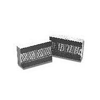
DISPLAY DOT MATRIX 32.77X20.07MM 5X7 RED
Manufacturer
Avago Technologies US Inc.
Series
HDLx-3416r
Datasheet
1.HDLO-3416.pdf
(12 pages)
Specifications of HDLO-3416
Character Format
Dot Matrix
Character Size
6.9mm
Led Color
Red
Luminous Intensity
3.5mcd
No. Of Digits / Alpha
4
Display Area Width
32.77mm
Display Area Height
10.16mm
Millicandela Rating
*
Internal Connection
*
Size / Dimension
1.29" x 0.79" (32.77mm x 20.07mm)
Color
Red
Configuration
*
Voltage - Forward (vf) Typ
*
Package / Case
22-DIP
Display Type
Alphanumeric
Number Of Digits/alpha
4
Digit/alpha Size
0.27" (6.86mm)
Number Of Digits
4
Illumination Color
Red
Wavelength
626 nm
Operating Voltage
- 0.5 V to 7 V
Maximum Operating Temperature
+ 85 C
Minimum Operating Temperature
- 40 C
Lead Free Status / RoHS Status
Lead free / RoHS Compliant
Common Pin
-
Lead Free Status / Rohs Status
Details


7
Electrical Description
Pin Function
Chip Enable (CE
CE
Clear (CLR, Pin 5)
Cursor Enable
(CUE Pin 11)
Cursor Select
(CU, Pin 10)
Write (WR, Pin 9)
Address Inputs
(A
7 and 8)
Data Inputs (D
Pins 16 – 22)
V
GND (Pin 12)
Blanking Input
(BL, Pin 14)
DD
1
2
, Pins 3 and 4)
and A
(Pin 6)
0
, Pins
0
-D
1
and
6
,
Description
CE
When CLR is a logic 0 the ASCII RAM is reset to
20hex (space) and the Control Register/Attribute
RAM is reset to 00hex.
CUE determines whether the IC displays the ASCII or
the Cursor memory. (1 = Cursor, 0 = ASCII.)
CU determines whether data is stored in the ASCII
RAM or the Attribute RAM/Control Register.
(1 = ASCII, 0 = Attribute RAM/ Control Register.)
WR must be a logic 0 to store data in the display.
A
memory. Address 00 accesses the far right display
location. Address 11 accesses the far left location.
D
the display.
V
GND is the display ground.
BL is used to flash the display, blank the
display or to dim the display.
0
DD
0
-A
-D
1
and CE
is the positive power supply input.
1
6
are used to specify the input data for
selects a specific location in the display
2
must be a logic 0 to write to the display.
Display Internal Block Diagram
Figure 1 shows the HDLX-3416
display internal block diagram.
The CMOS IC consists of a 4 x 7
Character RAM, a 2 x 4 Attribute
RAM, a 5 bit Control Register, a
128 character ASCII decoder
and the refresh circuitry
necessary to synchronize the
decoding and driving of four 5 x
7 dot matrix displays.
Four 7 bit ASCII words are
stored in the Character RAM.
The IC reads the ASCII data and
decodes it via the 128 character
ASCII decoder. The ASCII
decoder includes the 64
character set of the HPDL-2416,
32 lower case ASCII symbols,
and 32 foreign language
symbols.
A 5 bit word is stored in the
Control Register. Three fields
within the Control Register
provide an 8 level brightness
control, master blank, and
extended functions disable.
For each display digit location,
two bits are stored in the
Attribute RAM. One bit is used
to enable a cursor character at
each digit location. A second bit
is used to individually disable
the blanking features at each
digit location.
The display is blanked and
dimmed through an internal
blanking input on the row
drivers. Logic within the IC
allows the user to dim the
display either through the BL
input or through the brightness
control in the control register.
Similarly the display can be
blanked through the BL input,
the Master Blank in the Control
Register, or the Digit Blank
Disable in the Attribute RAM.
Related parts for HDLO-3416
Image
Part Number
Description
Manufacturer
Datasheet
Request
R

Part Number:
Description:
LED DISPLAY 5X7 5MM 4CHAR HE RED
Manufacturer:
Avago Technologies US Inc.
Datasheet:

Part Number:
Description:
DISPLAY 5X7 0.15" 4CHAR RED
Manufacturer:
Avago Technologies US Inc.
Datasheet:

Part Number:
Description:
DISPLAY DOT MATRIX 25.15X20.07MM 5X7 RED
Manufacturer:
Avago Technologies US Inc.
Datasheet:

Part Number:
Description:
OPTOCOUPLER GATE DRV 2A 16-SOIC
Manufacturer:
Avago Technologies US Inc.
Datasheet:
Part Number:
Description:
OPTOCOUPLER 2CH 2.5A 16-SOIC
Manufacturer:
Avago Technologies US Inc.
Datasheet:

Part Number:
Description:
OPTOCOUPLER GATE DRV 0.4A 16SOIC
Manufacturer:
Avago Technologies US Inc.
Datasheet:

Part Number:
Description:
OPTOCOUPLER 2.0A 250KHZ 8-DIP
Manufacturer:
Avago Technologies US Inc.
Datasheet:

Part Number:
Description:
OPTOCOUPLER 2.0A 250KHZ GW 8-SMD
Manufacturer:
Avago Technologies US Inc.
Datasheet:

Part Number:
Description:
OPTOCOUPLER 2CH 15MBD 3.3V 8SOIC
Manufacturer:
Avago Technologies US Inc.
Datasheet:
Part Number:
Description:
OPTOCOUPLER DARL-OUT 8-DIP
Manufacturer:
Avago Technologies US Inc.
Datasheet:
Part Number:
Description:
OPTOCOUPLER IGBT DRIVE 0.4A 8DIP
Manufacturer:
Avago Technologies US Inc.
Datasheet:
Part Number:
Description:
OPTOCOUPLER DARL-OUT 8-DIP
Manufacturer:
Avago Technologies US Inc.
Datasheet:

Part Number:
Description:
OPTOCOUPLER 1CH 1MBS 8-SMD GW
Manufacturer:
Avago Technologies US Inc.
Datasheet:
Part Number:
Description:
OPTOCOUPLER GATE DRIVER 8-DIP
Manufacturer:
Avago Technologies US Inc.
Datasheet:

Part Number:
Description:
OPTOCOUPLER GATE DRIVER 8-SMD
Manufacturer:
Avago Technologies US Inc.
Datasheet: