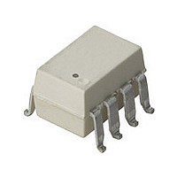
ACPL-J313-300E Avago Technologies US Inc., ACPL-J313-300E Datasheet - Page 15

ACPL-J313-300E
Manufacturer Part Number
ACPL-J313-300E
Description
Gate Drive Optocoupler,SMD+LF
Manufacturer
Avago Technologies US Inc.
Datasheet
1.ACPL-3130-500E.pdf
(20 pages)
Specifications of ACPL-J313-300E
Voltage - Isolation
3750Vrms
Number Of Channels
1, Unidirectional
Current - Output / Channel
2.5A
Propagation Delay High - Low @ If
300ns @ 10mA ~ 16mA
Current - Dc Forward (if)
25mA
Input Type
DC
Output Type
Push-Pull, Totem-Pole
Mounting Type
Surface Mount
Package / Case
8-SMD Gull Wing
Number Of Elements
1
Forward Voltage
1.95V
Forward Current
25mA
Isolation Voltage
3750Vrms
Package Type
PDIP SMD
Operating Temp Range
-40C to 100C
Power Dissipation
295mW
Propagation Delay Time
500ns
Pin Count
8
Mounting
Surface Mount
Reverse Breakdown Voltage
5V
Operating Temperature Classification
Industrial
Lead Free Status / RoHS Status
Lead free / RoHS Compliant
Lead Free Status / RoHS Status
Lead free / RoHS Compliant
Applications Information
Eliminating Negative IGBT Gate Drive (Discussion applies to
ACPL-3130, ACPL-J313, and ACNW3130)
To keep the IGBT firmly off, the ACPL-3130 has a very
low maximum VOL specification of 0.5 V. The ACPL-3130
realizes this very low V
with 1 W (typical) on resistance in its pull down circuit.
When the ACPL-3130 is in the low state, the IGBT gate is
shorted to the emitter by R
the lead inductance from the ACPL-3130 to the IGBT gate
and emitter (possibly by mounting the ACPL-3130 on a
small PC board directly above the IGBT) can eliminate the
need for negative IGBT gate drive in many applications as
shown in Figure 29. Care should be taken with such a PC
board design to avoid routing the IGBT collector or emitter
traces close to the ACPL-3130 input as this can result in
unwanted coupling of transient signals into the ACPL-
3130 and degrade performance. (If the IGBT drain must
be routed near the ACPL-3130 input, then the LED should
be reverse-biased when in the off state, to prevent the
transient signals coupled from the IGBT drain from turning
on the ACPL-3130.)
Figure 29. Recommended LED Drive and Application Circuit.
CONTROL
Figure 30. ACPL-3130 Typical Application Circuit with Negative IGBT Gate Drive.
5
CONTROL
COLLECTOR
COLLECTOR
INPUT
INPUT
+5 V
+5 V
74XXX
74XXX
OPEN
OPEN
270 Ω
270
OL
1
2
3
4
1
2
3
4
by using a DMOS transistor
g
+ 1 W. Minimizing R
8
7
6
5
0.1 µF
g
8
7
6
5
and
0.1 µF
Selecting the Gate Resistor (R
Losses. (Discussion applies to ACPL-3130, ACPL-J313 and
ACNW3130)
Step 1: Calculate Rg minimum from the I
IGBT and R
with a voltage supplied by the ACPL-3130.
The V
conservative value of V
Figure 6). At lower R
ACPL-3130 is not an ideal voltage step. This results in
lower peak currents (more margin) than predicted by this
analysis. When negative gate drive is not used V
previous equation is equal to zero volts.
+
-
+
-
V
V
+
-
CC
EE
Rg
V
CC
= 15 V
= -5 V
OL
Rg
R
= 18 V
value of 2 V in the previous equation is a
g
g
Q1
Q2
≥
in Figure 30 can be analyzed as a simple RC circuit
V
=
=
Q1
Q2
CC
15
7.2Ω
−
I
OLPEAK
+
2.5
V
EE
5
∼
=
−
−
g
8Ω
2
values the voltage supplied by the
V
OL
OL
at the peak current of 2.5A (see
g
) to Minimize IGBT Switching
3-PHASE
+ HVDC
- HVDC
OL
AC
peak specification. The
3-PHASE
+ HVDC
- HVDC
AC
EE
in the


