ACPL-J313-300E Avago Technologies US Inc., ACPL-J313-300E Datasheet - Page 7
ACPL-J313-300E
Manufacturer Part Number
ACPL-J313-300E
Description
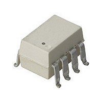
Gate Drive Optocoupler,SMD+LF
Manufacturer
Avago Technologies US Inc.
Datasheet
1.ACPL-3130-500E.pdf
(20 pages)
Specifications of ACPL-J313-300E
Voltage - Isolation
3750Vrms
Number Of Channels
1, Unidirectional
Current - Output / Channel
2.5A
Propagation Delay High - Low @ If
300ns @ 10mA ~ 16mA
Current - Dc Forward (if)
25mA
Input Type
DC
Output Type
Push-Pull, Totem-Pole
Mounting Type
Surface Mount
Package / Case
8-SMD Gull Wing
Number Of Elements
1
Forward Voltage
1.95V
Forward Current
25mA
Isolation Voltage
3750Vrms
Package Type
PDIP SMD
Operating Temp Range
-40C to 100C
Power Dissipation
295mW
Propagation Delay Time
500ns
Pin Count
8
Mounting
Surface Mount
Reverse Breakdown Voltage
5V
Operating Temperature Classification
Industrial
Lead Free Status / RoHS Status
Lead free / RoHS Compliant
Lead Free Status / RoHS Status
Lead free / RoHS Compliant


Table 1. IEC/EN/DIN EN 60747-5-2 Insulation Characteristics*
* Refer to the optocoupler section of the Isolation and Control Components Designer’s Catalog, under Product Safety Regulations section, (IEC/EN/DIN
EN 60747-5-2) for a detailed description of Method a and Method b partial discharge test profiles.
Note: These optocouplers are suitable for “safe electrical isolation” only within the safety limit data. Maintenance of the safety data shall be ensured by
means of protective circuits. Surface mount classification is Class A in accordance with CECC 00802.
Table 2. Insulation and Safety Related Specifications
All Avago data sheets report the creepage and clearance inherent to the optocoupler component itself. These dimensions are needed as a starting
point for the equipment designer when determining the circuit insulation requirements. However, once mounted on a printed circuit board, minimum
creepage and clearance requirements must be met as specified for individual equipment standards. For creepage, the shortest distance path along
the surface of a printed circuit board between the solder fillets of the input and output leads must be considered. There are recommended techniques
such as grooves and ribs which may be used on a printed circuit board to achieve desired creepage and clearances. Creepage and clearance distances
will also change depending on factors such as pollution degree and insulation level.
Description
Installation classification per DIN VDE 0110/1.89, Table 1
for rated mains voltage �� 150 V
for rated mains voltage �� 300 V
for rated mains voltage �� 450 V
for rated mains voltage �� 600 V
for rated mains voltage �� 1000 V
Climatic Classification
Pollution Degree (DIN VDE 0110/1.89)
Maximum Working Insulation Voltage
Input to Output Test Voltage, Method b* V
100% Production Test with t
Input to Output Test Voltage, Method a* V
Type and Sample Test, t
Highest Allowable Overvoltage
(Transient Overvoltage tini = 10 sec)
Safety-limiting values – maximum values allowed in the event of a
failure, also see Figure 41 and 42.
Case Temperature
Input Current
Output Power
Insulation Resistance at T
Parameter
Minimum External Air
Gap (Clearance)
Minimum External
Tracking (Creepage)
Minimum Internal
Plastic Gap (Internal
Clearance)
Tracking Resistance
(Comparative Tracking
Index)
Isolation Group
m
=60 sec, Partial discharge < 5 pC
Symbol
L(101)
L(102)
CTI
S
, V
�� 150 V
�� 300 V
�� 450 V
�� 600 V
�� 1000 V
m
150 V
300 V
450 V
600 V
1000 V
IO
=1 sec, Partial discharge < 5 pC
= 500 V
rms
rms
rms
rms
ACPL-3130
7.1
7.4
0.08
> 175
IIIa
rms
IORM
IORM
x 1.5=V
x 1.875=V
ACPL-J313
7.4
8.0
0.5
> 175
IIIa
PR
,
PR
,
ACNW3130
9.6
10.0
1.0
> 200
IIIa
P
I
S, OUTPUT
Symbol
S, INPUT
V
V
V
V
IORM
IOTM
R
Units
mm
mm
mm
V
T
PR
PR
S
S
Option 060
55/100/21
ACPL-3130
Conditions
Measured from input terminals to output
terminals, shortest distance through air.
Measured from input terminals to output
terminals, shortest distance path along body.
Through insulation distance conductor to
conductor, usually the straight line distance
thickness between the emitter and detector.
DIN IEC 112/VDE 0303 Part 1
Material Group (DIN VDE 0110, 1/89, Table 1)
1181
6000
>10
I – IV
I – IV
I – III
630
945
175
230
600
2
9
55/100/21 55/100/21
ACPL-J313
I – IV
I – IV
1670
1336
6000
>10
I – III
I – III
891
175
400
600
2
9
ACNW3130
1414
2652
2121
8000
>10
I – IV
I – IV
I – IV
I – IV
I – III
150
400
700
2
9
V
V
V
V
Unit
mW
mA
peak
peak
peak
peak
°C
W
Related parts for ACPL-J313-300E
Image
Part Number
Description
Manufacturer
Datasheet
Request
R

Part Number:
Description:
OPTOCOUPLER GATE DVR 2.5A 8-DIP
Manufacturer:
Avago Technologies US Inc.
Datasheet:
Part Number:
Description:
Gate Drive Optocoupler, T/R+LF
Manufacturer:
Avago Technologies US Inc.
Datasheet:

Part Number:
Description:
OPTOCOUPLER GATE DRV 2A 16-SOIC
Manufacturer:
Avago Technologies US Inc.
Datasheet:
Part Number:
Description:
OPTOCOUPLER 2CH 2.5A 16-SOIC
Manufacturer:
Avago Technologies US Inc.
Datasheet:

Part Number:
Description:
OPTOCOUPLER GATE DRV 0.4A 16SOIC
Manufacturer:
Avago Technologies US Inc.
Datasheet:

Part Number:
Description:
OPTOCOUPLER 2.0A 250KHZ 8-DIP
Manufacturer:
Avago Technologies US Inc.
Datasheet:

Part Number:
Description:
OPTOCOUPLER 2.0A 250KHZ GW 8-SMD
Manufacturer:
Avago Technologies US Inc.
Datasheet:

Part Number:
Description:
OPTOCOUPLER 2CH 15MBD 3.3V 8SOIC
Manufacturer:
Avago Technologies US Inc.
Datasheet:
Part Number:
Description:
OPTOCOUPLER DARL-OUT 8-DIP
Manufacturer:
Avago Technologies US Inc.
Datasheet:
Part Number:
Description:
OPTOCOUPLER IGBT DRIVE 0.4A 8DIP
Manufacturer:
Avago Technologies US Inc.
Datasheet:
Part Number:
Description:
OPTOCOUPLER DARL-OUT 8-DIP
Manufacturer:
Avago Technologies US Inc.
Datasheet:

Part Number:
Description:
OPTOCOUPLER 1CH 1MBS 8-SMD GW
Manufacturer:
Avago Technologies US Inc.
Datasheet:
Part Number:
Description:
OPTOCOUPLER GATE DRIVER 8-DIP
Manufacturer:
Avago Technologies US Inc.
Datasheet:

Part Number:
Description:
OPTOCOUPLER GATE DRIVER 8-SMD
Manufacturer:
Avago Technologies US Inc.
Datasheet:

Part Number:
Description:
OPTOCOUPLER PHOTOTRANS 4-SMD
Manufacturer:
Avago Technologies US Inc.
Datasheet: