ADNS-3060 Avago Technologies US Inc., ADNS-3060 Datasheet - Page 11
ADNS-3060
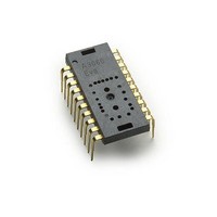
Manufacturer Part Number
ADNS-3060
Description
Optical Mouse Sensor,DIP
Manufacturer
Avago Technologies US Inc.
Datasheet
1.ADNS-3060.pdf
(38 pages)
Specifications of ADNS-3060
Lead Free Status / RoHS Status
Lead free / RoHS Compliant
Lead Free Status / RoHS Status
Lead free / RoHS Compliant
Other names
Q2073278B


AC Electrical Specifications
Electrical Characteristics over recommended operating conditions. Typical values at 25 °C, V
11
Parameter
VDD to RESET
Data delay after
RESET
Input delay after
reset
Power Down
Wake from NPD
Data delay after
NPD
RESET pulse width
MISO rise time
MISO fall time
MISO delay after
SCLK
MISO hold time
MOSI hold time
MOSI setup time
SPI time between
write commands
SPI time between
write and read com-
mands
SPI time between
read and subse-
quent commands
SPI read address-
data delay
SPI motion read ad-
dress-data delay
NCS to SCLK active
SCLK to NCS inac-
tive
NCS to MISO high-Z
SROM download
and frame capture
byte-to-byte delay
NCS to burst mode
exit
Transient Supply
Current
Symbol
t
t
T
t
t
t
t
t
t
t
t
t
t
t
t
t
t
t
t
t
t
t
t
I
DDT
OP
PU-RESET
PD
PUPD
COMPUTE
PW-RESET
r-MISO
f-MISO
DLY-MISO
hold-MISO
hold-MOSI
setup-MOSI
SWW
SWR
SRW
SRAD
SRAD-MOT
NCS-SCLK
SCLK-NCS
NCS-MISO
LOAD
BEXIT
IN-RST
t
SRR
Minimum Typical
10
250
200
120
50
50
250
50
75
120
120
10
4
40
40
Maximum Units Notes
250
35
500
2.1
75
3.1
200
200
120
85
250
Ps
ms
Ps
ms
ms
ms
Ps
ns
ns
ns
ns
ns
ns
Ps
Ps
ns
Ps
Ps
ns
ns
ns
Ps
Ps
mA
From VDD = 3.0V to RESET sampled
From RESET falling edge to valid motion data at
2000 fps and shutter bound 8290.
From RESET falling edge to inputs active (NPD,
MOSI, NCS, SCLK)
From NPD falling edge to initiate the power down
cycle at 500fps (tpd = 1 frame period + 100ms )
From NPD rising edge to valid motion data at
2000 fps and shutter bound 8290. Max assumes
surface change while NPD is low.
From NPD rising edge to all registers contain data
from new images at 2000fps (see Figure 10) .
C
C
From SCLK falling edge to MISO data valid, no load
conditions
Data held until next falling SCLK edge
Amount of time data is valid after SCLK rising edge
From data valid to SCLK rising edge
From rising SCLK for last bit of the first data byte,
to rising SCLK for last bit of the second data byte.
From rising SCLK for last bit of the first data byte,
to rising SCLK for last bit of the second address
byte.
From rising SCLK for last bit of the first data byte,
to falling SCLK for first bit of the second address
byte.
From rising SCLK for last bit of the address byte,
to falling SCLK for first bit of data being read. All
registers except Motion & Motion_Burst
From rising SCLK for last bit of the address byte, to
falling SCLK for first bit of data being read. Applies
to 0x02 Motion, and 0x50 Motion_Burst, registers
From NCS falling edge to first SCLK rising edge
From last SCLK falling edge to NCS rising edge, for
valid MISO data transfer
From NCS rising edge to MISO high-Z state
(see Figure 23 and 24)
Time NCS must be held high to exit burst mode
Max supply current during a V
3.6V
L
L
= 50pF
= 50pF
DD3
=3.3V, fclk=24MHz.
DD3
ramp from 0 to
Related parts for ADNS-3060
Image
Part Number
Description
Manufacturer
Datasheet
Request
R

Part Number:
Description:
Optical Mouse Sensor,DIP
Manufacturer:
Avago Technologies US Inc.
Datasheet:

Part Number:
Description:
Optical Mouse Sensor,DIP
Manufacturer:
Avago Technologies US Inc.
Datasheet:

Part Number:
Description:
Trim Lens For ADNS-3530
Manufacturer:
Avago Technologies US Inc.
Datasheet:

Part Number:
Description:
8 DIP SFF Navigation Sensor
Manufacturer:
Avago Technologies US Inc.
Datasheet:

Part Number:
Description:
Trim Lens For ADNS-5090
Manufacturer:
Avago Technologies US Inc.
Datasheet:

Part Number:
Description:
BLACK CLIP FOR ADNS-5000
Manufacturer:
Avago Technologies US Inc.
Datasheet:
Part Number:
Description:
Lens For ADNS-7630
Manufacturer:
Avago Technologies US Inc.
Datasheet:

Part Number:
Description:
Optical Mouse Sensor,DIP
Manufacturer:
Avago Technologies US Inc.
Datasheet:

Part Number:
Description:
SENSOR OPTICAL MOUSE 8-DIP
Manufacturer:
Avago Technologies US Inc.
Datasheet:
Part Number:
Description:
Optical Mouse Sensor,DIP
Manufacturer:
Avago Technologies US Inc.
Datasheet:

Part Number:
Description:
OPTOCOUPLER GATE DRV 2A 16-SOIC
Manufacturer:
Avago Technologies US Inc.
Datasheet:
Part Number:
Description:
OPTOCOUPLER 2CH 2.5A 16-SOIC
Manufacturer:
Avago Technologies US Inc.
Datasheet:

Part Number:
Description:
OPTOCOUPLER GATE DRV 0.4A 16SOIC
Manufacturer:
Avago Technologies US Inc.
Datasheet:

Part Number:
Description:
OPTOCOUPLER 2.0A 250KHZ 8-DIP
Manufacturer:
Avago Technologies US Inc.
Datasheet:

Part Number:
Description:
OPTOCOUPLER 2.0A 250KHZ GW 8-SMD
Manufacturer:
Avago Technologies US Inc.
Datasheet: