IPR-QDRII/UNI Altera, IPR-QDRII/UNI Datasheet
IPR-QDRII/UNI
Specifications of IPR-QDRII/UNI


Related parts for IPR-QDRII/UNI


IPR-QDRII/UNI Summary of contents
Page 1
... User Guide External Memory Interface Handbook Volume 3 Section III. QDR II and QDR II+ SRAM Controller with 101 Innovation Drive San Jose, CA 95134 www.altera.com EMI_QDRII_UG-2.1 UniPHY User Guide Document last updated for Altera Complete Design Suite version: Document publication date: 10.1 December 2010 Subscribe ...
Page 2
... Altera warrants performance of its semiconductor products to current specifications in accordance with Altera’s standard warranty, but reserves the right to make changes to any products and services at any time without notice. Altera assumes no responsibility or liability arising out of the application or use of any information, product, or service described herein except as expressly agreed to in writing by Altera. Altera customers are advised to obtain the latest version of device specifications before relying on any published information and before placing orders for products or services ...
Page 3
... Advanced PHY Settings . . . . . . . . . . . . . . . . . . . . . . . . . . . . . . . . . . . . . . . . . . . . . . . . . . . . . . . . . . . . . . . 3–1 Topology . . . . . . . . . . . . . . . . . . . . . . . . . . . . . . . . . . . . . . . . . . . . . . . . . . . . . . . . . . . . . . . . . . . . . . . . . . . . 3–2 Controller Settings . . . . . . . . . . . . . . . . . . . . . . . . . . . . . . . . . . . . . . . . . . . . . . . . . . . . . . . . . . . . . . . . . . . . 3–2 Memory Parameters . . . . . . . . . . . . . . . . . . . . . . . . . . . . . . . . . . . . . . . . . . . . . . . . . . . . . . . . . . . . . . . . . . . . . 3–2 Memory Timing . . . . . . . . . . . . . . . . . . . . . . . . . . . . . . . . . . . . . . . . . . . . . . . . . . . . . . . . . . . . . . . . . . . . . . . . . 3–3 Board Settings . . . . . . . . . . . . . . . . . . . . . . . . . . . . . . . . . . . . . . . . . . . . . . . . . . . . . . . . . . . . . . . . . . . . . . . . . . 3–4 Intersymbol Interference . . . . . . . . . . . . . . . . . . . . . . . . . . . . . . . . . . . . . . . . . . . . . . . . . . . . . . . . . . . . . . . 3–4 December 2010 Altera Corporation External Memory Interface Handbook Volume 3 Section III. QDR II and QDR II+ SRAM Controller with UniPHY User Guide Contents ...
Page 4
... Example Driver Add-Ons . . . . . . . . . . . . . . . . . . . . . . . . . . . . . . . . . . . . . . . . . . . . . . . . . . . . . . . . . . . . . . 7–4 User Refresh Generator . . . . . . . . . . . . . . . . . . . . . . . . . . . . . . . . . . . . . . . . . . . . . . . . . . . . . . . . . . . . . . 7–4 Refresh Monitor . . . . . . . . . . . . . . . . . . . . . . . . . . . . . . . . . . . . . . . . . . . . . . . . . . . . . . . . . . . . . . . . . . . . 7–4 Data Corrupter . . . . . . . . . . . . . . . . . . . . . . . . . . . . . . . . . . . . . . . . . . . . . . . . . . . . . . . . . . . . . . . . . . . . . 7–4 Chapter 8. Latency Variable Controller Latency . . . . . . . . . . . . . . . . . . . . . . . . . . . . . . . . . . . . . . . . . . . . . . . . . . . . . . . . . . . . . . . 8–1 External Memory Interface Handbook Volume 3 Section III. QDR II and QDR II+ SRAM Controller with UniPHY User Guide Contents December 2010 Altera Corporation ...
Page 5
... Contents Chapter 9. Timing Diagrams Additional Information Document Revision History . . . . . . . . . . . . . . . . . . . . . . . . . . . . . . . . . . . . . . . . . . . . . . . . . . . . . . . . . . . Info–1 How to Contact Altera . . . . . . . . . . . . . . . . . . . . . . . . . . . . . . . . . . . . . . . . . . . . . . . . . . . . . . . . . . . . . . . . Info–1 Typographic Conventions . . . . . . . . . . . . . . . . . . . . . . . . . . . . . . . . . . . . . . . . . . . . . . . . . . . . . . . . . . . . . Info–2 December 2010 Altera Corporation External Memory Interface Handbook Volume 3 Section III. QDR II and QDR II+ SRAM Controller with UniPHY User Guide v ...
Page 6
... External Memory Interface Handbook Volume 3 Section III. QDR II and QDR II+ SRAM Controller with UniPHY User Guide Contents December 2010 Altera Corporation ...
Page 7
... ALTDQ_DQS megafunctions, available in the Quartus II software, but you then must consider all of the aspects of the design including timing analysis and design constraints. The UniPHY IP offers the Altera PHY interface (AFI). The AFI results in a simple connection between the PHY and controller. Release Information Table 1– ...
Page 8
... Device Family Support IP cores provide the following levels of support for target Altera device families: For FPGA device support: ■ Preliminary—verified with preliminary timing models for this device ■ Final—verified with final timing models for this device ■ ■ ...
Page 9
... Table 1–4. Unsupported Features for the QDR II and QDR II+ SRAM Controllers with UniPHY Memory Protocol QDR II SRAM QDR II+ SRAM MegaCore Verification Altera has carried out extensive random, directed tests with functional test coverage using industry-standard models to ensure the functionality of the QDR II and QDR II+ SRAM controllers with UniPHY. December 2010 Altera Corporation Key Feature ...
Page 10
... Altera verifies that the current version of the Quartus II software compiles the previous version of each MegaCore function. The and Errata report any exceptions to this verification. Altera does not verify compilation with MegaCore function versions older than one release. Resource Utilization This section lists resource utilization for the QDR II and QDR II+ SRAM controllers with UniPHY for supported device families ...
Page 11
... This chapter provides a general overview of the Altera IP core design flow to help you quickly get started with any Altera IP core. The Altera IP Library is installed as part of the Quartus II installation process. You can select and parameterize any Altera IP core from the library. Altera provides an integrated parameter editor that allows you to customize IP cores to support a wide variety of applications ...
Page 12
... Altera's Qsys system integration tool is now available as beta for evaluation in the Quartus II software subscription edition version 10.1. Altera does not recommend using the beta release of Qsys in the Quartus II software version 10.1 for designs that are close to completion and are meeting design requirements ...
Page 13
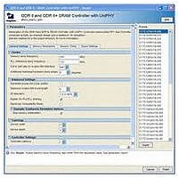
... Tools menu, and follow the prompts in the MegaWizard Plug-In Manager interface to create or edit a custom IP core variation select a specific Altera IP core, click the IP core in the Installed Plug-Ins list in the MegaWizard Plug-In Manager. 4. Specify the parameters on the Parameter Settings pages. For detailed explanations of these parameters, refer to the “ ...
Page 14
... For a complete list of models or libraries required to simulate your IP core, refer to the scripts provided with the testbench. For more information about simulating Altera IP cores, refer to Designs in volume 3 of the Quartus II Handbook. External Memory Interface Handbook Volume 3 Section III ...
Page 15
... SOPC Builder defines default connections, which you can modify. The HDL files are ready to be compiled by the Quartus II software to produce output files for programming an Altera device. SOPC Builder generates a simulation testbench module for supported cores that includes basic transactions to validate the HDL files ...
Page 16
... Some IP cores provide preset parameters for specific applications. If you wish to use preset parameters, click the arrow to expand the Presets list, select the desired preset, and then click Apply. To modify preset settings text editor edit the <installation directory>\ip\altera\uniphy\lib\<IP core>.qprs file. 1 ...
Page 17
... During system generation, you can specify whether SOPC Builder generates a simulation model and testbench for the entire system, which you can use to easily simulate your system in any of Altera's supported simulation tools. SOPC Builder also generates a set of ModelSim the testbench and plain-text RTL design files that describe your system in the ModelSim simulation software ...
Page 18
... Presets list, select the desired preset, and then click Apply. To modify preset settings text editor edit the <installation directory>\ip\altera\uniphy\lib\<IP core>.qprs file. 5. Click Finish to complete the IP core instance and add it to the system. ...
Page 19
... During system generation, Qsys generates a functional simulation model—or example design that includes a testbench—which you can use to simulate your system in any Altera-supported simulation tool. f For information about the latest Altera-supported simulation tools, refer to the Quartus II Software Release f For general information about simulating Altera IP cores, refer to Designs in volume 3 of the Quartus II Handbook ...
Page 20
... Signals that the Nios II code memory is Input being loaded from the external ROM. Remains asserted throughout initialization and becomes inactive when initialization Output is complete. soft_reset_n can be issued after hc_rom_config_init_busy is deasserted. December 2010 Altera Corporation Guide. For ...
Page 21
... Figure 2–5. HardCopy UnIPHY Example Design Memory Table 2–2 summarizes the DLL reconfiguration ports exposed at the top level of the Controller+PHY. Table 2–2. DLL Reconfiguration Ports Exposed at Top-Level of Controller+PHY Wrapper (Part 1 of hc_dll_config_dll_offset_ctrl_ addnsub December 2010 Altera Corporation Direction Output Output HardCopy Example Design AFI MM-Slave PHY ...
Page 22
... PLL is ready to act on a possible second adjustment pulse. The data output of the serial scan chain. Asserted when the scan chain write operation is in progress and is deasserted when the write operation is complete. December 2010 Altera Corporation ...
Page 23
... Note to Table 2–4: (1) <stamp> unique identifier determined by the MegaWizard Plug-in Manager at generation time. December 2010 Altera Corporation HardCopy III Device I/O Features HardCopy IV Device I/O Features File Name QIP file which refers to all generated files in the synthesis fileset ...
Page 24
... QIP which refers to UniPHY RTL in this fileset. This is distinct from ../<variation_name>.qip. This file is included automatically in the example project. UniPHY top-level wrapper. UniPHY Verilog RTL files. UniPHY SystemVerilog RTL fies. Synopsys constraints file. December 2010 Altera Corporation Chapter 2: Getting Started Generated Files Description Description Description ...
Page 25
... December 2010 Altera Corporation File Name‘ Pin Planner file. Pin constraints script to be run after synthesis. Other Tcl scripts. Readme text file. Example design project file. Example design project settings file. ...
Page 26
... UniPHY top-level wrapper. (1) UniPHY Verilog RTL files. (1) UniPHY SystemVerilog RTL files. (1) Synopsys constraints file. (1) Pin Planner file. Pin constraints script to be run (1) after synthesis. (1) Other Tcl scripts. (1) Readme text file. December 2010 Altera Corporation Chapter 2: Getting Started Generated Files Description Description ...
Page 27
... Note to Table 2–11: (1) <stamp> unique identifier created by Qsys during generation. December 2010 Altera Corporation File Name Other IP core files. File Name Qsys system top-level wrapper. UniPHY top-level wrapper. UniPHY Verilog RTL files. UniPHY SystemVerilog RTL files ...
Page 28
... External Memory Interface Handbook Volume 3 Section III. QDR II and QDR II+ SRAM Controller with UniPHY User Guide Chapter 2: Getting Started Generated Files December 2010 Altera Corporation ...
Page 29
... Generate power-of-2 bus widths Maximum Avalon-MM burst length I/O standard Master for PLL/DLL sharing December 2010 Altera Corporation Parameter The frequency of the clock that drives the memory device. The frequency of the clock that feeds the PLL. Defines the width of the data bus on the Avalon-MM interface ...
Page 30
... Specifies the number of clock cycles required for a request to pass through an idling controller. Parameter The width of the address bus on the memory device. The width of the data bus on the memory device. Chapter 3: Parameter Settings Memory Parameters Description Description Description Description December 2010 Altera Corporation ...
Page 31
... Internal jitter TCQHCQnH TKHKnH December 2010 Altera Corporation Parameter The width of the data-mask on the memory device, The width of the CQ (read strobe) bus on the memory device. The width of the K (write strobe) bus on the memory device. The burst length supported by the memory device. ...
Page 32
... The maximum skew between D and BWS signals referenced by a common K signal. The maximum skew between Q signals referenced by a common CQ signal. The maximum skew between CQ signals of different read data groups. Chapter 3: Parameter Settings Board Settings Description Description December 2010 Altera Corporation ...
Page 33
... K Average delay difference between write data signals and K Average delay difference between read data signals and CQ December 2010 Altera Corporation Parameter The maximum skew between the address/command signals. A value equal to the average of the longest and smallest address/command signal delay values, minus the delay of the K signal ...
Page 34
... External Memory Interface Handbook Volume 3 Section III. QDR II and QDR II+ SRAM Controller with UniPHY User Guide Chapter 3: Parameter Settings Board Settings December 2010 Altera Corporation ...
Page 35
... For more information about how to include your board simulation results in the Quartus II software and how to assign pins using pin planners, refer to Design Flow Tutorials December 2010 Altera Corporation 4. Constraining and Compiling of the External Memory Interface Handbook. External Memory Interface Handbook Volume 3 Section III ...
Page 36
... Compile the Design To compile the design, on the Processing menu, click Start Compilation. After you have compiled the top-level file, you can perform RTL simulation or program your targeted Altera device to verify the top-level file in hardware. f For more information about simulating, refer to the the External Memory Interface Handbook ...
Page 37
... The command-issuing full-state machine (FSM) has two states: INIT and INIT_COMPLETE. In the INIT_COMPLETE state, commands are issued immediately as requests arrive using combinational logic and do not require state transitions. December 2010 Altera Corporation 5. Functional Description—Controller Figure 5–1 shows a block diagram of the ...
Page 38
... Signals” on page Width Direction Avalon-MM Signal Type 1 Out waitrequest_n 1 In read ≤ address 1 Out readdatavalid Chapter 5: Functional Description—Controller Avalon-MM and Memory Data Width 6–1. Full-Rate Designs 2:1 4:1 6–10. Description — — — — December 2010 Altera Corporation ...
Page 39
... Avalon-MM slave write interface. Table 5–3. Avalon-MM Slave Write Signals Signal avl_w_ready avl_w_write_req avl_w_addr 18, 36, 72, 144 avl_w_wdata 2,4,8,16 avl_w_be log_2(MAX_BURST_SI avl_w_size December 2010 Altera Corporation Width Direction Avalon-MM Signal Type Out readdata — ZE Width Direction Avalon-MM Signal Type 1 ...
Page 40
... External Memory Interface Handbook Volume 3 Section III. QDR II and QDR II+ SRAM Controller with UniPHY User Guide Chapter 5: Functional Description—Controller Signal Description December 2010 Altera Corporation ...
Page 41
... External Memory Device I/O Pads The I/O pads contain all the I/O instantiations. The bulk of the UniPHY I/O circuitry is encapsulated in the ALTDQ_DQS megafunction (ALTDQ_DQS2 for Stratix V series devices). December 2010 Altera Corporation 6. Functional Description—UniPHY FPGA UniPHY Address and Command Datapath ...
Page 42
... Clocks address/command out to memory. Set in wizard 180° gives adress and command center Dual-regional (default 225°) aligned with memory clock; 225° produces best overall timing results. Chapter 6: Functional Description—UniPHY Block Description Description Description December 2010 Altera Corporation ...
Page 43
... In full-rate mode, ddio_address_h and ddio_addesss_l are the same. Figure 6–2. Address and Command Datapath afi_address pll_afi_clk addr_cmd_clk December 2010 Altera Corporation Clock Network Phase Type A continuous running clock from the 90° Local memory device for capturing read data ...
Page 44
... Section III. QDR II and QDR II+ SRAM Controller with UniPHY User Guide DDIO_OUT 0 DDIO_OUT n-1 HDR SDR Chapter 6: Functional Description—UniPHY Block Description vcc gnd phy_mem_clk wdata[0] DDIO_OUT wdata[1] 0 wdata[2] DDIO_OUT 1 wdata[3] wdata[4n-1:0] wdata[4n-4] DDIO_OUT wdata[4n-3] 2n-2 wdata[4n-2] DDIO_OUT wdata[4n-1] 2n-1 phy_afi_clk phy_mem_write_clk December 2010 Altera Corporation ...
Page 45
... Remain in this state until reset is released. LOAD_INIT Load any initialization values for simulation purposes. Wait until the memory device is stable. The QDR II and QDR II+ specification requires 2,048 STABLE cycles of power up wait time. December 2010 Altera Corporation DDIO_IN data_high data_low DDIO_IN_n-1 write enable ...
Page 46
... If latency counter value is smaller than predefined ideal condition minimum, then go to CALIB_FAIL. CALIB_DONE Calibration is successful. CALIB_FAIL Calibration is not successful. External Memory Interface Handbook Volume 3 Section III. QDR II and QDR II+ SRAM Controller with UniPHY User Guide Chapter 6: Functional Description—UniPHY Block Description December 2010 Altera Corporation ...
Page 47
... When you instantiate master and slave variants into your HDL code, you must connect the PLL outputs from the master to the clock inputs of the slaves. 1 The master .qip file must appear before the slave .qip file in the Quartus II Settings File (.qsf). December 2010 Altera Corporation UniPHY Top-Level File UniPHY OCT DLL ...
Page 48
... The DLL and PLL Sharing interface is not available with SOPC Builder. External Memory Interface Handbook Volume 3 Section III. QDR II and QDR II+ SRAM Controller with UniPHY User Guide Chapter 6: Functional Description—UniPHY Interfaces December 2010 Altera Corporation ...
Page 49
... Figure 6–7. PHY Architecture without Master for OCT Control Block Memory Interface RUP and RDN 1 The OCT Sharing Interface and OCT slave mode are not available with SOPC Builder. December 2010 Altera Corporation Figure 6–7, respectively, show the PHY architecture with and without UniPHY Top-Level File UniPHY ...
Page 50
... UniPHY Signals shows the clock and reset Description on the appropriate RUP ccio Description Half-rate or full-rate clock supplied to controller and system logic. Reset output on afi_clk clock domain. For use as asynchronous reset. This signal is asynchronously asserted and synchronously deasserted. December 2010 Altera Corporation ...
Page 51
... QDR II and QDR II+ SRAM interface signals. Table 6–6. QDR II and QDR II+ SRAM Interface Signals Name Output mem_address Output mem_bws_n Output mem_wps_n Output mem_rps_n Output mem_doff_n December 2010 Altera Corporation Direction Width MEM_ADDRESS_WIDTH 2 x MEM_ADDRESS_WIDTH 2 x MEM_ADDRESS_WIDTH MEM_CONTROL_WIDTH MEM_CONTROL_WIDTH MEM_DM_WIDTH × AFI_RATIO MEM_DQ_WIDTH × 2 × AFI_RATIO MEM_WRITE_DQS_ WIDTH × ...
Page 52
... Offset input setting for the DLL. This setting is a Gray-coded offset that is added or subtracted from the current value of the DLL’s delay chain. The registered and Gray-coded value of the current delay-offset setting. December 2010 Altera Corporation ...
Page 53
... The AFI bank width, derived from the corresponding memory interface width. AFI_BANK_WIDTH The AFI chip select width, derived from the corresponding memory interface width. AFI_CHIP_SELECT_WIDTH The AFI data mask width. AFI_DATA_MASK_WIDTH December 2010 Altera Corporation Direction Description Control signal to enable PLL Input reconfiguration. ...
Page 54
... Table 6–9. AFI New Signal Names afi_clk afi_reset_n External Memory Interface Handbook Volume 3 Section III. QDR II and QDR II+ SRAM Controller with UniPHY User Guide Table 6–9 AFI Name ctl_clk ctl_reset_n Chapter 6: Functional Description—UniPHY UniPHY Signals shows the renamed AFI Old Name December 2010 Altera Corporation ...
Page 55
... AFI. The AFI standardizes and simplifies the interface between controller and PHY for all Altera memory designs, thus allowing you to easily interchange your own controller code with Altera's high-performance controllers. The AFI PHY includes an administration block that configures the memory for calibration and performs necessary accesses to mode registers that configure the memory as required (these calibration processes are different) ...
Page 56
... Figure 6–9 shows a full-rate write. Figure 6–9. Full-Rate Write afi_clk afi_dqs_burst afi_wdata_valid afi_wdata External Memory Interface Handbook Volume 3 Section III. QDR II and QDR II+ SRAM Controller with UniPHY User Guide Chapter 6: Functional Description—UniPHY PHY-to-Controller Interfaces December 2010 Altera Corporation ...
Page 57
... Figure 6–11. Half-Rate Reads clock afi_addr AX XA afi_cs_n 10 afi_rdata_en 10 01 mem_dqs mem_dq afi_rdata_valid afi_rdata December 2010 Altera Corporation Figure 6–11 afi_rlat = afi_rlat = Section III. QDR II and QDR II+ SRAM Controller with UniPHY User Guide shows half-rate reads ...
Page 58
... External Memory Interface Handbook Volume 3 Section III. QDR II and QDR II+ SRAM Controller with UniPHY User Guide Figure 6–13 show writes and reads, where the data is written to and Figure 6–13 assume the following general points: Chapter 6: Functional Description—UniPHY PHY-to-Controller Interfaces December 2010 Altera Corporation ...
Page 59
... In all waveforms a command record is added that combines the memory pins ras_n, cas_n and we_n into the current command that is issued. This command is registered by the memory when chip select (mem_cs_n) is low. The important commands in the presented waveforms are WR = write, ACT = activate. December 2010 Altera Corporation Note 2 Note 4 ...
Page 60
... Observe the alignment of returned read data relative to data on the bus. External Memory Interface Handbook Volume 3 Section III. QDR II and QDR II+ SRAM Controller with UniPHY User Guide Note FFFFFFFF FFFFFFFF 00 0020008 RD Chapter 6: Functional Description—UniPHY PHY-to-Controller Interfaces Note 3 Note December 2010 Altera Corporation ...
Page 61
... Open the <variation_name>/<variation_name>_<stamp>_controller_phy.sv file. 3. Replace the <variation_name>_<stamp>_alt_qdr_controller module with your custom controller module. 4. Delete the ports of the Altera high-performance memory controller, and add the top-level ports of your custom controller. 5. Similarily, update the port names in the top-level module in the <variation_name>.v or <variation_name>.vhd file. ...
Page 62
... If you intend to run simulation from the Quartus II software, ensure that the .qip file points to the vendor-supplied memory model. External Memory Interface Handbook Volume 3 Section III. QDR II and QDR II+ SRAM Controller with UniPHY User Guide Chapter 6: Functional Description—UniPHY Using a Vendor-Specific Memory Model December 2010 Altera Corporation ...
Page 63
... This block is available in Verilog HDL only. Figure 7–1 shows the testbench and the example top-level file. Figure 7–1. Testbench and Example Top-Level File Testbench December 2010 Altera Corporation 7. Functional Description—Example Example Top-Level File Controller with Example Driver UniPHY Section III ...
Page 64
... External Memory Interface Handbook Volume 3 Section III. QDR II and QDR II+ SRAM Controller with UniPHY User Guide Chapter 7: Functional Description—Example Top-Level Project December 2010 Altera Corporation Example Driver ...
Page 65
... Table 7–1. Driver Signals (Part Signal clk reset_n avl_ready avl_write_req avl_read_req avl_addr avl_size avl_wdata avl_rdata avl_rdata_valid pnf_per_bit pnf_per_bit_ persist December 2010 Altera Corporation Width Signal Type avl_ready avl_write_req avl_read_req 24 avl_addr 3 avl_size 72 avl_wdata 72 avl_rdata avl_rdata_valid pnf_per_bit ...
Page 66
... Throughout the four types of error injection tests, the data corrupter exercises a walking-one pattern to confirm correctness. External Memory Interface Handbook Volume 3 Section III. QDR II and QDR II+ SRAM Controller with UniPHY User Guide Chapter 7: Functional Description—Example Top-Level Project Width Signal Type pass fail test_complete Example Driver December 2010 Altera Corporation ...
Page 67
... The data corrupter is created when you turn on Enable Error Detection Parity under Controller Settings on the General Settings tab of the parameter editor. The data corrupter resides in data_corrupter.sv in the rtl_sim subdirectory. December 2010 Altera Corporation External Memory Interface Handbook Volume 3 Section III. QDR II and QDR II+ SRAM Controller with UniPHY User Guide ...
Page 68
... External Memory Interface Handbook Volume 3 Section III. QDR II and QDR II+ SRAM Controller with UniPHY User Guide Chapter 7: Functional Description—Example Top-Level Project December 2010 Altera Corporation Example Driver ...
Page 69
... Altera defines read and write latencies in terms of memory clock cycles. These latencies apply to supported device families types of latencies that exists while designing with memory controllers—read and write latencies, which have the following definitions: ■ Read latency—the amount of time it takes for the read data to appear at the local interface after initiating the read request. Write latency— ...
Page 70
... Controller Settings section of the General Settings tab of the QDR II and QDR II+ SRAM controller with UniPHY parameter editor. External Memory Interface Handbook Volume 3 Section III. QDR II and QDR II+ SRAM Controller with UniPHY User Guide Chapter 8: Latency Variable Controller Latency December 2010 Altera Corporation ...
Page 71
... You can set the avl_w_size to 0x2 and hold avl_w_addr constant at 0x0 to perform the same back-to-back write. Figure 9–1. Back-to-Back Writes Figure 9–2 shows back-to-back read from addresses 0 and 1. December 2010 Altera Corporation 9. Timing Diagrams External Memory Interface Handbook Volume 3 Section III. QDR II and QDR II+ SRAM Controller with UniPHY User Guide ...
Page 72
... You can set the avl_w_size to 0x2 and hold avl_w_addr constant at 0x0 to perform the same back-to-back read. Figure 9–2. Back-to-Back Reads External Memory Interface Handbook Volume 3 Section III. QDR II and QDR II+ SRAM Controller with UniPHY User Guide Chapter 9: Timing Diagrams December 2010 Altera Corporation ...
Page 73
... Contact Technical support Technical training Product literature Non-technical support (General) (Software Licensing) Note to Table: (1) You can also contact your local Altera sales office or sales representative. December 2010 Altera Corporation Changes Device Family Support, Features list, and Design Flows, added new ...
Page 74
... A warning calls attention to a condition or possible situation that can cause you injury. The envelope links to the Email Subscription Management Center website, where you can sign up to receive update notifications for Altera documents. Chapter : Typographic Conventions page of the Altera December 2010 Altera Corporation ...