RS08KA2 PROMO Freescale Semiconductor, RS08KA2 PROMO Datasheet - Page 3
RS08KA2 PROMO
Manufacturer Part Number
RS08KA2 PROMO
Description
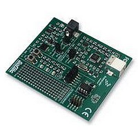
DEMO KIT, SILICON BUNDLE, RS08KA2
Manufacturer
Freescale Semiconductor
Datasheet
1.RS08KA2_PROMO.pdf
(34 pages)
Specifications of RS08KA2 PROMO
Kit Contents
DEMO9RS08KA2 Board, USB Cable, Quick Start Guide, User Manual, Packing List
Svhc
No SVHC (15-Dec-2010)
Development Tool Type
Demonstration Kit
Kit Features
RS08KA2 Microcontroller,
Silicon Manufacturer
Freescale
Core Architecture
RS08
Core Sub-architecture
RS08
Silicon Core Number
MC9RS08
Silicon Family Name
RS08KA
Rohs Compliant
Yes
Lead Free Status / RoHS Status
Lead free / RoHS Compliant


The 8-bit general purpose accumulator A provides a primary data register for the RS08 CPU. Data can be
read from memory into A with the LDA instruction. The data in A can be written into memory with the
STA instruction. The new added exchange instructions, SHA and SLA, allow values to be exchanged
between accumulator A and shadow program counter (SPC) high byte and low byte respectively.
The program counter (PC) contains the address of the next instruction or operand to be fetched as in the
HC08/S08 platform. However, the PC in RS08 platform is 14-bit long, which means the maximum
addressable space is 16K bytes.
In HC08/S08 platform, the return PC value is stacked into RAM during subroutine calls using JSR and
BSR instructions. In RS08 platform, RAM stacking mechanism is eliminated, return address is saved into
the SPC register. Upon completion of the subroutine, RTS instruction will restore the content of the PC
from SPC. SPC only provides a single level of address saving, nested subroutine calls can be performed
through software stacking. User firmware can utilize SHA and SLA instructions to swap the high byte and
the low byte content of SPC to A, then stack them to RAM.
The status bits (Z and C) in condition code register (CCR) indicates the results of previous arithmetic and
other operations. The bit definition is identical as in HC08/S08 platform. Please refer to RS08 Core
Reference Manual for their detail definition.
1.1.2
In additional to the CPU registers, there are two memory mapped registers that are tightly coupled with
the core address generation. They are the indirect data register (D[X]) and the index register (X). These
registers are located at $000E and $000F respectively.
Registers D[X] and X together perform indirect data access. The register X contains the address which is
used when register D[X] is accessed.
registers are not part of the CPU internal registers, but they are integrated seamlessly with the RS08
generic instruction set to form a pseudo instruction set.
Freescale Semiconductor
Special Registers
Figure 1-2. RS08 Special Registers
Figure 1-3
INDIRECT DATA REGISTER D[X] (location $000E)
Getting Started with RS08, Rev. 1
7
7
INDEX REGISTER
shows the index addressing scheme. The X and D[X]
0
0
X (location $000F)
Introduction to RS08
3
Related parts for RS08KA2 PROMO
Image
Part Number
Description
Manufacturer
Datasheet
Request
R

Part Number:
Description:
Manufacturer:
Freescale Semiconductor, Inc
Datasheet:
Part Number:
Description:
Manufacturer:
Freescale Semiconductor, Inc
Datasheet:
Part Number:
Description:
Manufacturer:
Freescale Semiconductor, Inc
Datasheet:
Part Number:
Description:
Manufacturer:
Freescale Semiconductor, Inc
Datasheet:
Part Number:
Description:
Manufacturer:
Freescale Semiconductor, Inc
Datasheet:
Part Number:
Description:
Manufacturer:
Freescale Semiconductor, Inc
Datasheet:
Part Number:
Description:
Manufacturer:
Freescale Semiconductor, Inc
Datasheet:
Part Number:
Description:
Manufacturer:
Freescale Semiconductor, Inc
Datasheet:
Part Number:
Description:
Manufacturer:
Freescale Semiconductor, Inc
Datasheet:
Part Number:
Description:
Manufacturer:
Freescale Semiconductor, Inc
Datasheet:
Part Number:
Description:
Manufacturer:
Freescale Semiconductor, Inc
Datasheet:
Part Number:
Description:
Manufacturer:
Freescale Semiconductor, Inc
Datasheet:
Part Number:
Description:
Manufacturer:
Freescale Semiconductor, Inc
Datasheet:
Part Number:
Description:
Manufacturer:
Freescale Semiconductor, Inc
Datasheet:
Part Number:
Description:
Manufacturer:
Freescale Semiconductor, Inc
Datasheet: