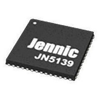
JN5139/001,531 NXP Semiconductors, JN5139/001,531 Datasheet - Page 32

JN5139/001,531
Manufacturer Part Number
JN5139/001,531
Description
MCU 802.15.4 32BIT 2.4G 56-QFN
Manufacturer
NXP Semiconductors
Datasheet
1.JN5139-Z01-V.pdf
(82 pages)
Specifications of JN5139/001,531
Frequency
2.4GHz
Modulation Or Protocol
802.15.4
Applications
General Purpose
Power - Output
*
Sensitivity
-96dBm
Voltage - Supply
2.7 V ~ 3.6 V
Current - Receiving
37mA
Current - Transmitting
37mA
Data Interface
PCB, Surface Mount
Memory Size
96kB RAM, 192kB ROM
Antenna Connector
PCB, Surface Mount
Operating Temperature
-20°C ~ 70°C
Package / Case
56-VFQFN
Core
RISC
Lead Free Status / RoHS Status
Lead free / RoHS Compliant
The data transfer rate on the SPI bus is determined by the SPICLK signal. The JN5139 supports transfers at
selectable data rates from 16MHz to 250kHz selected by a clock divider. Both SPICLK clock phase and polarity are
configurable. The clock polarity controls if SCLK is high or low between transfers (and hence the polarity of the first
clock edge in a transfer). The clock phase and polarity determines which edge of SPICLK is used by the JN5139 to
present new data on the SPIMOSI line; the opposite edge will be used to read data from the SPIMISO line. The
interface should be configured appropriately for the SPI slave being accessed.
If more than one SPISEL line is to be used in a system they must be used in numerical order, for instance if 3 SPI
select lines are to be used, they must be SPISEL0, 1 and 2. A SPISEL line can be configured to automatically
deassert between transactions if required, or it may stay asserted over a number of transactions. For devices such
as memories where a large amount of data can be received by the master by continually providing SPICLK
transitions, the ability for the select line to stay asserted is an advantage since it keeps the slave enabled over the
whole of the transfer.
32
Polarity
(CPOL)
0
0
1
1
SPICLK
(CPHA)
Phase
Memory
Slave 0
Flash
0
1
0
1
Mode
0
1
2
3
Figure 23: Typical JN5139 SPI Peripheral Connection
SPISEL0
Slave 1
Defined
Description
SPICLK is low when idle – the first edge is positive.
Valid data is output on SPIMOSI before the first clock and changes every
negative edge. SPIMISO is sampled every positive edge.
SPICLK is low when idle – the first edge is positive.
Valid data is output on SPIMOSI every positive edge. SPIMISO is sampled every
negative edge.
SPICLK is high when idle – the first edge is negative.
Valid data is output on SPIMOSI before the first clock edge and is changed
every positive edge. SPIMISO is sampled every negative edge.
SPICLK is high when idle – the first edge is negative.
Valid data is output on SPIMOSI every negative edge. SPIMISO is sampled
every positive edge.
User
JN5139
SPISEL1
SPISEL2
Table 3 SPI Configurations
SPISEL3
JN-DS-JN5139 1v9
SPISEL4
Slave 2
Defined
User
36
33
34
SPIMOSI
SPICLK
SPIMISO
Slave 3
Defined
User
© NXP Laboratories UK 2010
Slave 4
Defined
User


