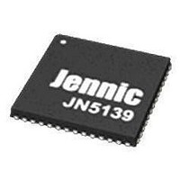
JN5139/001,531 NXP Semiconductors, JN5139/001,531 Datasheet - Page 34

JN5139/001,531
Manufacturer Part Number
JN5139/001,531
Description
MCU 802.15.4 32BIT 2.4G 56-QFN
Manufacturer
NXP Semiconductors
Datasheet
1.JN5139-Z01-V.pdf
(82 pages)
Specifications of JN5139/001,531
Frequency
2.4GHz
Modulation Or Protocol
802.15.4
Applications
General Purpose
Power - Output
*
Sensitivity
-96dBm
Voltage - Supply
2.7 V ~ 3.6 V
Current - Receiving
37mA
Current - Transmitting
37mA
Data Interface
PCB, Surface Mount
Memory Size
96kB RAM, 192kB ROM
Antenna Connector
PCB, Surface Mount
Operating Temperature
-20°C ~ 70°C
Package / Case
56-VFQFN
Core
RISC
Lead Free Status / RoHS Status
Lead free / RoHS Compliant
11 Intelligent Peripheral Interface
The Intelligent Peripheral (IP) Interface is provided for systems that are more complex, where there is a processor
that requires a wireless peripheral. As an example, the JN5139 may provide a complete JenNet wireless network
interface to a phone, computer, PDA, set-top box or games console. No resources are required from the main
processor compared to a transceiver as the complete wireless protocol may be run on the internal JN5139 CPU. The
wireless peripheral may be controlled via one of the UARTs but the IP interface is intended to provide a high-speed,
low-processor-overhead interface. The IP interface cannot be used with the CPU in doze.
The intelligent peripheral interface is a SPI slave interface and uses pins shared with other DIO signals. The
interface is designed to allow message passing and data transfer. Data received and transmitted on the IP interface
is copied directly to and from a dedicated area of memory without intervention from the CPU. This memory area, the
intelligent peripheral memory block, contains 64 32-bit word receive and transmit buffers.
The interface functions as a SPI slave. It is possible to select the clock edge of IP_CLK on which data on the IP_DIN
line of the interface is sampled, and the state of data output IP_DOUT is changed. The order of transmission is MSB
first. The IP_DO data output is tri-stated when the device is inactive, i.e. the device is not selected via IP_SEL. An
interrupt output line IP_INT is available so that the JN5139 can indicate to an external master that it has data to
transfer. The interface can be clocked at up to 8MHz.
The IP interface signals IP_CLK, IP_DO, IP_DI, IP_SEL, IP_INT are alternate functions of pins DIO14 to 18
respectively.
11.1 Data Transfer Format
Transfers are started by the remote processor asserting the IP_SEL line and terminated by the remote processor de-
asserting IP_SEL.
Data transfers are bi-directional and traffic in both directions has a format of status byte, data length byte (of the
number of 32-bit words to transfer) and data packet (from the receive and transmit buffers), as shown in Figure 25.
The first byte transferred into the JN5139 is a status byte with the format shown in Table 4. This is followed by a
padding byte that should be set to zero. The first byte output by the JN5139 is a padding byte, that should be ignored,
followed by a status byte with the format shown in Table 4
If data is queued for transmission and the recipient has indicated that they are ready for it (RXRDY in incoming status
byte was 1), the next byte to be transmitted is the data length in words. If either the JN5139 or the remote processor
has no data to transfer, then the data length should be set to zero. The transaction can be terminated by the master
after the status and padding bytes have been sent if it is not possible to send data in either direction. This may be
34
7:2
1
0
Bit
RSVD
TXQ
RXRDY
Field
Peripheral
Intelligent
Interface
JN5139
Reserved, set to 0.
1: Data queued for transmission
1: Buffer ready to receive data
Figure 24: Intelligent Peripheral Connection
IP_DO
IP_INT
IP_DI
IP_SEL
IP_CLK
Table 4: IP Status Byte Format
JN-DS-JN5139 1v9
SPIMISO
SPIMOSI
SPISEL
SPICLK
SPIINT
Description
(e.g. in cellphone, computer)
MASTER
SPI
System Processor
© NXP Laboratories UK 2010
CPU


