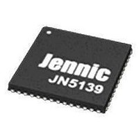
JN5139/001,531 NXP Semiconductors, JN5139/001,531 Datasheet - Page 37

JN5139/001,531
Manufacturer Part Number
JN5139/001,531
Description
MCU 802.15.4 32BIT 2.4G 56-QFN
Manufacturer
NXP Semiconductors
Datasheet
1.JN5139-Z01-V.pdf
(82 pages)
Specifications of JN5139/001,531
Frequency
2.4GHz
Modulation Or Protocol
802.15.4
Applications
General Purpose
Power - Output
*
Sensitivity
-96dBm
Voltage - Supply
2.7 V ~ 3.6 V
Current - Receiving
37mA
Current - Transmitting
37mA
Data Interface
PCB, Surface Mount
Memory Size
96kB RAM, 192kB ROM
Antenna Connector
PCB, Surface Mount
Operating Temperature
-20°C ~ 70°C
Package / Case
56-VFQFN
Core
RISC
Lead Free Status / RoHS Status
Lead free / RoHS Compliant
An interrupt can be generated when the counter is equal to the value in either of the High or Low registers.
The internal Output Enable (OE) signal enables or disables the timer output.
The Timer 0 signals CK_GT, CAP and OUT are alternative functions of pins DIO8, 9 and 10 respectively and Timer 1
signals CK_GT, CAP and OUT are alternative functions of pins DIO11, 12, and 13 respectively. Selection of either
the Timer or DIOx functionality is made through software, in either case the timer still functions internally.
Note, timer 0 may only be used internally when an external 32kHz clock source is used.
12.1.1 Pulse Width Modulation Mode
Pulse Width Modulation (PWM) mode allows the user to specify an overall cycle time and pulse length within the
cycle. The pulse can be generated either as a single shot or as a train of pulses with a repetition rate determined by
the cycle time.
In this mode, the cycletime and low periods of the PWM output signal can be set by the values of two independent
16-bit registers (Fall and Rise). The counter increments and its output is compared to the 16-bit Rise and Fall
registers. When the counter is equal to the Rise register, the PWM output is set to high; when the counter reaches
the Fall value, the output returns to low. In continuous mode, when the counter reaches the Fall value, it will reset
and the cycle repeats. The PWM waveform is available on TIMxOUT when the output driver is enabled.
Rise
Fall
Figure 27: PWM Output Timings
12.1.2 Capture Mode
The capture mode can be used to measure the time between transitions of a signal applied to the capture input
(TIMxCAP). When the capture is started, on the next low-to-high transition of the captured signal, the count value is
stored in the Rise register, and on the following high-to-low transition, the counter value is stored in the Fall register.
The pulse width is the difference in counts in the two registers multiplied by the period of the prescaled clock . Upon
reading the capture registers the counter is stopped. The values in the High and Low registers will be updated
whenever there is a corresponding transition on the capture input, and the value stored will be relative to when the
mode was started. Therefore, if multiple pulses are seen on TIMxCAP before the counter is stopped only the last
pulse width will be stored.
9
5
3
4
CLK
CAPT
t
t
RISE
RISE
t
FALL
Capture Mode Enabled
Rise
x
9
3
Fall
x
14
7
Figure 28: Capture Mode
© NXP Laboratories UK 2010
JN-DS-JN5139 1v9
37


